Embedded type multifunctional integrated structure and method for manufacturing the same

a multifunctional integrated structure and embedded technology, applied in the direction of cross-talk/noise/interference reduction, circuit electrostatic discharge protection, transportation and packaging, etc., can solve the problems of occupying many space of electronic products, waste of methods of prior art, etc., to increase the function of embedded multifunctional integrated structure, reduce the size of passive components, reduce the effect of solder joints

Inactive Publication Date: 2009-05-21
INPAQ TECH
View PDF7 Cites 71 Cited by
  • Summary
  • Abstract
  • Description
  • Claims
  • Application Information

AI Technical Summary

Benefits of technology

[0006]One particular aspect of the present invention is to provide an embedded type multifunctional integrated structure and a method for manufacturing the same. The present invention utilizes the concept of multi-layer design to integrated more than two passive components on a component structure that would be adhered to a substrate. Hence, the embedded type multifunctional integrated structure has an OCP (Over-Current Protection) function, an OVP (Over-Voltage Protection) function, an anti-EMI (anti-Electromagnetic Interference) function, and an anti-ESD (anti-Electrostatic Discharge) function at the same time. Therefore, the present invention effectively integrated two or more than one passive components in order to increase function of the embedded type multifunctional integrated structure. Moreover, the present invention effectively reduces the size of the passive components on a PCB and reduces the number of solder joints.

Problems solved by technology

However, each pass component only has a single function in the prior design.
Therefore, the method of the prior art wastes cost and occupies many space of the electronic product.

Method used


Image

  • Embedded type multifunctional integrated structure and method for manufacturing the same
  • Embedded type multifunctional integrated structure and method for manufacturing the same
  • Embedded type multifunctional integrated structure and method for manufacturing the same

Examples


first embodiment

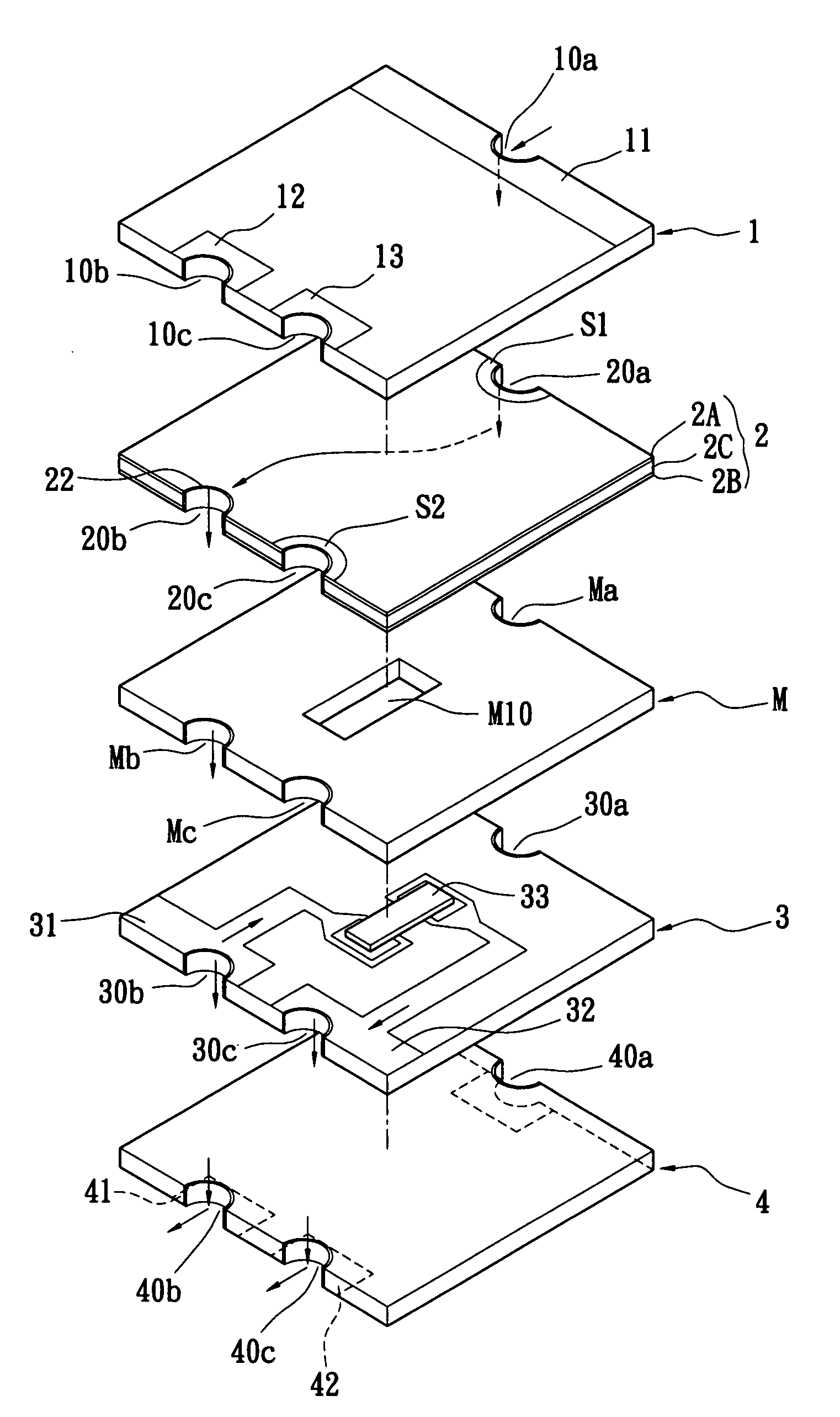
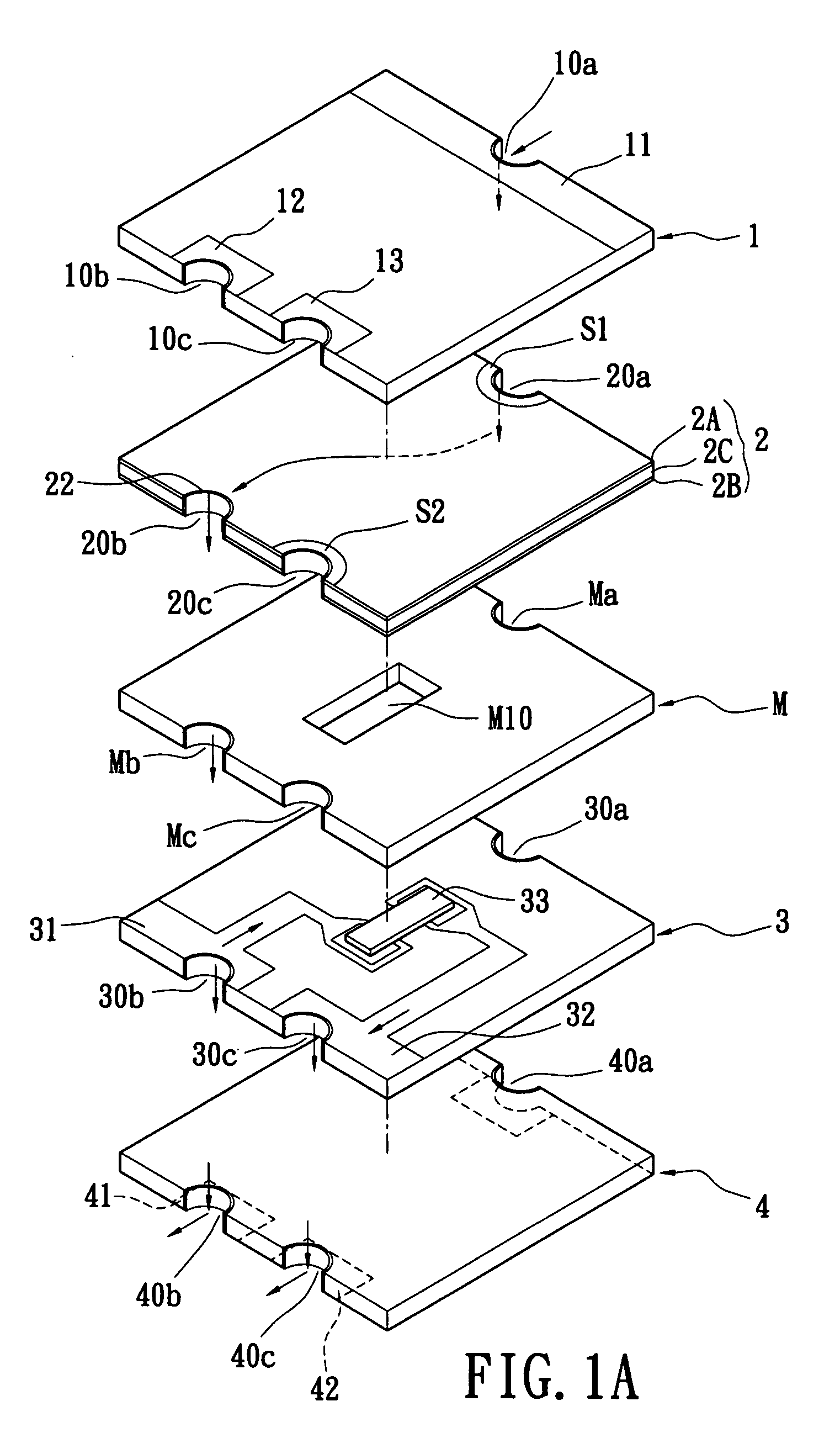
[0028]Referring to above-mentioned figures, the present invention provides an embedded type multifunctional integrated structure that includes a top cover insulating layer 1, a over-current protection layer 2, a middle insulating layer M, a multifunctional protection layer 3, a bottom cover insulating layer 4, and a lateral conductive unit 5. Moreover, the top cover insulating layer 1, the over-current protection layer 2, the middle insulating layer M, the multifunctional protection layer 3, and the bottom cover insulating layer 4 are stacked together in sequence. The lateral conductive unit 5 has a first lateral conductive layer 51, a second lateral conductive layer 52, and a third lateral conductive layer 53 insulated from each other.

[0029]In addition, the top cover insulating layer 1 has a first half hole 10a formed on a lateral side thereof, and a second half hole 10b and a third half hole 10c respectively formed on an opposite lateral side thereof. The top cover insulating laye...

second embodiment

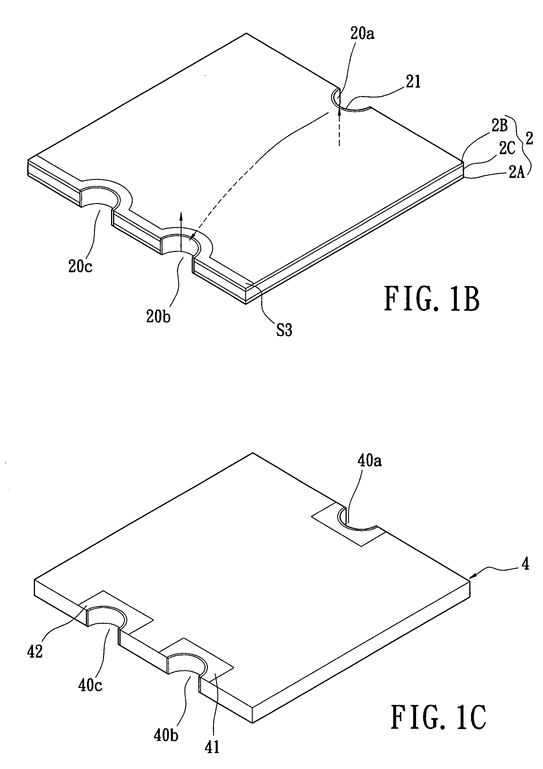
[0050]Therefore, the current path of second layer (the over-current protection layer 2′) of the second embodiment is that the current flows through the first electrode layer 2A′, the positive temperature coefficient material layer 2C′, and the second electrode layer 2B′ in sequence and flows from the second power input portion 21′ to the second power output portion 22′.

[0051]Referring to FIGS. 3A and 3B, FIG. 3A shows a perspective view of a multifunctional protection layer according to the third embodiment of the present; FIG. 3B shows a reversed, perspective view of a multifunctional protection layer according to the third embodiment of the present. The third power input portion 31′, the third power output portion 32′, and the multifunctional chip unit 33′ are formed on a bottom surface of the multifunctional protection layer 3′. In addition, the bottom cover insulating layer 4′ has an opening 40′ for receiving the multifunctional chip unit 33′.

[0052]Furthermore, the present inven...


PUM

PropertyMeasurementUnit
voltageaaaaaaaaaa
conductiveaaaaaaaaaa
poweraaaaaaaaaa

Abstract

An embedded type multifunctional integrated structure and a method for manufacturing the same are disclosed. The present invention utilizes the concept of multi-layer design to integrated more than two passive components on a component structure that would be adhered to a substrate. Hence, the embedded type multifunctional integrated structure has an OCP function, an OVP function, an anti-EMI function, and an anti-ESD function at the same time. Therefore, the present invention effectively integrated two or more than one passive components in order to increase function of the embedded type multifunctional integrated structure. Moreover, the present invention effectively reduces the size of the passive components on a PCB and reduces the number of solder joints.

Description

BACKGROUND OF THE INVENTION[0001]1. Field of the Invention[0002]The present invention relates to a multifunctional integrated structure and a method for manufacturing the same, and particularly relates to an embedded type multifunctional integrated structure and a method for manufacturing the same.[0003]2. Description of the Related Art[0004]For future electronic product, the electronic product design tends to achieve the functions of light, thin, short, and small. Moreover, the size of the passive components is larger than that of other electronic components in the electronic product. Hence, if the passive components can be effectively integrated together, the electronic product can achieve the functions of light, thin, short, and small easily.[0005]However, each pass component only has a single function in the prior design. Hence, when a designer needs to use many different functions for protecting the electronic product, the designer only can place many pass components with a sin...

Claims


Application Information

Patent Timeline
Patent Type & Authority Applications(United States)
IPC IPC(8): B32B5/00B05D5/12
CPCH05K1/0234H05K1/0257H05K1/0259H05K1/141H05K1/167H05K1/185Y10T428/239H05K3/4611H05K3/4688H05K2201/09181H05K2201/09309H05K2201/10045H05K3/3442
Inventor HUANG, CHIEN-HAOLI, WEN-CHIH
Owner INPAQ TECH
Why Eureka
Try Eureka