Liquid crystal display device

a liquid crystal display and display device technology, applied in the field of liquid crystal display devices, can solve the problems of flickering on the screen, uneven image quality, and inability to achieve the effect of achieving the effect of achieving the effect of achieving the effect of achieving the effect of achieving the effect of achieving the effect of achieving the effect of achieving the effect of achieving the effect of achieving the effect of achieving the effect of achieving the effect of achieving the effect of achieving the effect o

Active Publication Date: 2009-05-28
FUNAI ELECTRIC CO LTD
View PDF11 Cites 38 Cited by
  • Summary
  • Abstract
  • Description
  • Claims
  • Application Information

AI Technical Summary

Benefits of technology

[0034]It is obvious that such a more specific configuration produces the

Problems solved by technology

Nonuniform common voltage Vcom that is applied to the counter electrode results in nonuniformity in the drive voltage Vd per pixel applied to the liquid crystal layer and gives rise to a flicker in the screen and uneven image quality.
However, this method is not practicable, because the larger the wire diameter, the smaller will be the aperture ratio of the glass substrate.
However, the impedance of the c

Method used


Image

  • Liquid crystal display device
  • Liquid crystal display device
  • Liquid crystal display device

Examples


first embodiment

1. FIRST EMBODIMENT

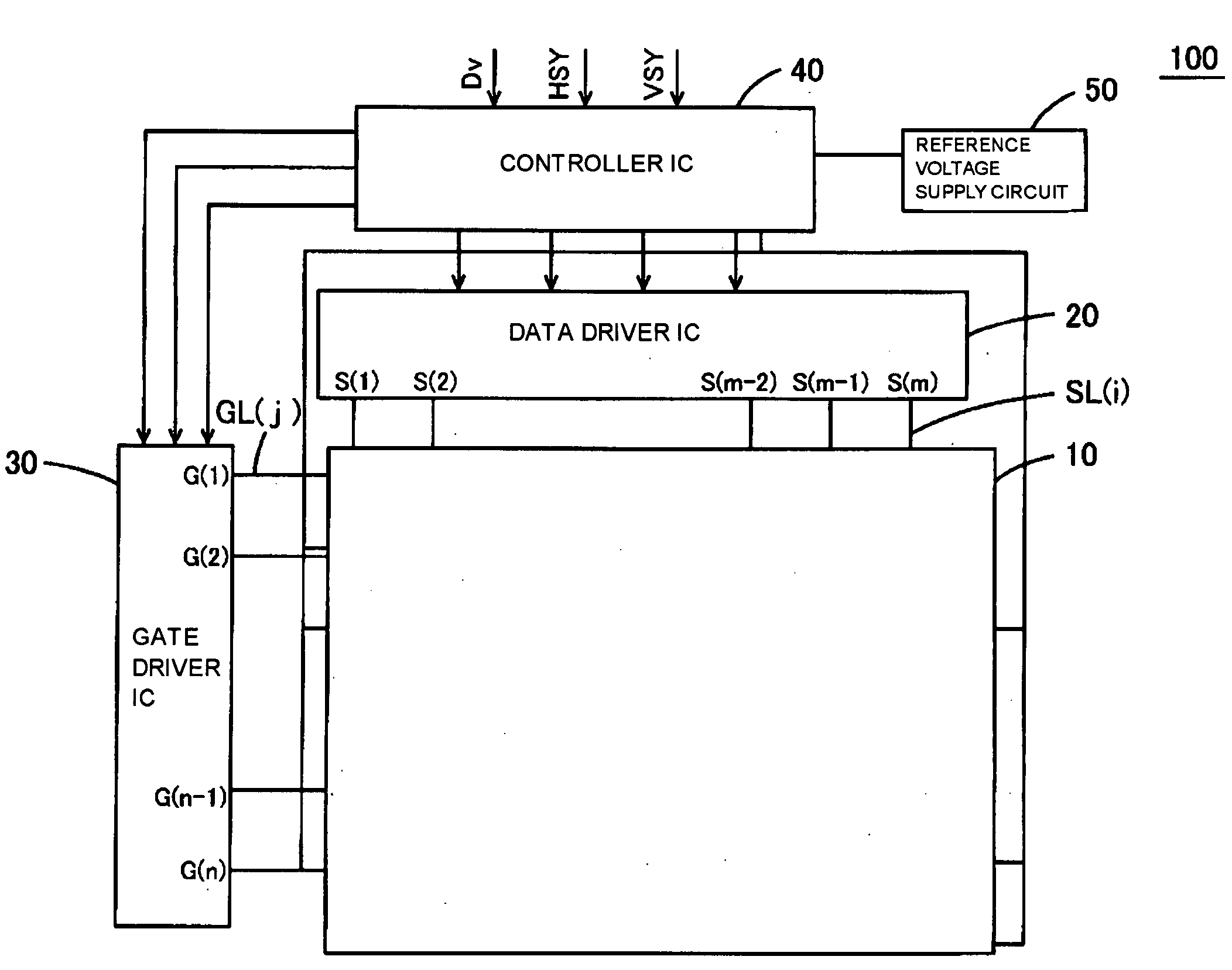
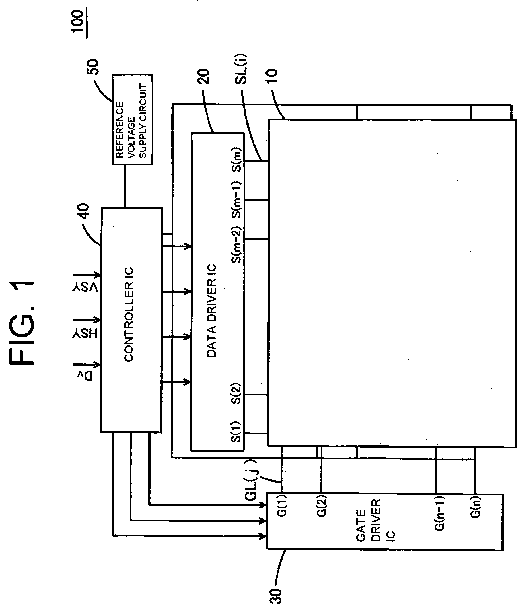
[0051]1.1 Structure of Liquid Crystal Display Device

[0052]A liquid crystal display device according to a first embodiment of the invention generates a drive voltage Vd based on an image signal (video signal and synchronization signal) supplied. Application of the generated drive voltage Vd to pixels varies the light transmittance across the pixels and an image is displayed by the multiple pixels having different transmittance values. The liquid crystal display device carries out feedback control of a common voltage Vcom serving as a reference for the drive voltage Vd, thereby avoiding nonuniformity in a displayed image and enhancing display quality. The following description of the present embodiment assumes that the liquid crystal display device is an active matrix type. However, the present invention can be applied to any liquid crystal display device that uses a common voltage Vcom to drive liquid crystal, even adopting any other driving method.

[0053]FIG. 1 is ...

second embodiment

2. SECOND EMBODIMENT

[0076]In the foregoing first embodiment, feedback control of a common voltage Vcom value for a certain subset of pixels P (i, j) is performed using one operational amplifier. However, in a case where a larger counter electrode is used as in a liquid crystal display device for a large screen, the LCD device may be adapted to implement Vcom feedback control individually in a plurality of areas of the counter electrode using a plurality of operational amplifiers.

[0077]FIG. 11 is a block diagram of a liquid crystal display device 100. This device has the same structure as shown in FIG. 1, though the gate driver IC is omitted from FIG. 11 for the sake of simplicity. Operational amplifiers 44 to 46 are responsible for feedback control of a common voltage Vcom that is applied in both lateral marginal areas and a virtually center area of the counter electrode 15. In particular, the operational amplifier 44 feedback controls the common voltage Vcom applied in an area T2 o...


PUM


Abstract

The liquid crystal display device 100 has a matrix arrangement of pixels which are formed by a liquid crystal layer, display electrodes disposed across the liquid crystal layer, and a counter electrode made of a transparent material and represents a tone (gray scale level) per pixel by applying a drive voltage to the liquid crystal layer, the drive voltage corresponding to a potential difference between each of the display electrodes and the counter electrode. The device also includes a common voltage supplying part 42 that detects a charge in a certain area T1 of the counter electrode 15 and compares a feedback voltage corresponding to the detected charge in the area, thereby providing common voltage Vcom feedback control. Consequently, flickers on the screen can be prevented by common voltage Vcom feedback control.

Description

CROSS REFERENCE TO RELATED APPLICATIONS[0001]The present application is related to the Japan Utility Model Application No. 2007-306473, filed Nov. 27, 2007, the entire disclosure of which is expressly incorporated by reference herein.BACKGROUND OF THE INVENTION[0002]1. Field of the Invention[0003]The present invention relates to a liquid crystal display device and, particularly, to such device in which the charge on a counter electrode is controlled not to vary.[0004]2. Description of the Related Art[0005]A liquid crystal display device displays an image by means of liquid crystal. The liquid crystal display device includes an upper glass substrate, a lower glass substrate, and a liquid crystal layer sandwiched between these substrates. Of the upper glass substrate, on its under surface facing the liquid crystal layer, a counter electrode for applying a common voltage Vcom to the liquid crystal layer and a transmission line X for supplying the common voltage Vcom to the counter elec...

Claims


Application Information

Patent Timeline
IPC IPC(8): G09G3/36
CPCG09G3/3655G09G3/3696G09G2320/0233G09G2320/0204G09G2320/0223G09G2300/043
Inventor NAKATSUKA, HITOSHI
Owner FUNAI ELECTRIC CO LTD
Why Eureka
Try Eureka