Display apparatus and fabrication method and fabrication apparatus for the same

a technology of display apparatus and fabrication method, which is applied in the manufacture of electric discharge tubes/lamps, lighting and heating apparatus, instruments, etc., can solve the problems of obstructing the reduction of the yield drop, and the efficiency percentage of the display apparatus is not improved, so as to improve the efficiency percentage of the display apparatus and reduce the cost of the display apparatus. , the effect of yield drop

Active Publication Date: 2009-05-28
JOLED INC
View PDF3 Cites 24 Cited by
  • Summary
  • Abstract
  • Description
  • Claims
  • Application Information

AI Technical Summary

Benefits of technology

[0019]However, if dust or the like sticks, upon fabrication of a panel, to an electro-optical element beginning with an organic EL element, then the electro-optical element becomes a dark spot element which does not emit light normally and forms a pixel de

Problems solved by technology

However, if dust or the like sticks, upon fabrication of a panel, to an electro-optical element beginning with an organic EL element, then the electro-optical element becomes a dark spot element which does not emit light normally and forms a pixel defect on the panel, and this makes a cause of a drop of the yield.
Such a defect to display as just described makes an obstacle to improvement of the efficiency percentage of the display apparatus and obstructs reduction of the cost of the

Method used


Image

  • Display apparatus and fabrication method and fabrication apparatus for the same
  • Display apparatus and fabrication method and fabrication apparatus for the same
  • Display apparatus and fabrication method and fabrication apparatus for the same

Examples


Embodiment Construction

[0082]Hereinafter, an embodiment of the present invention will be described with reference to the accompanying drawings.

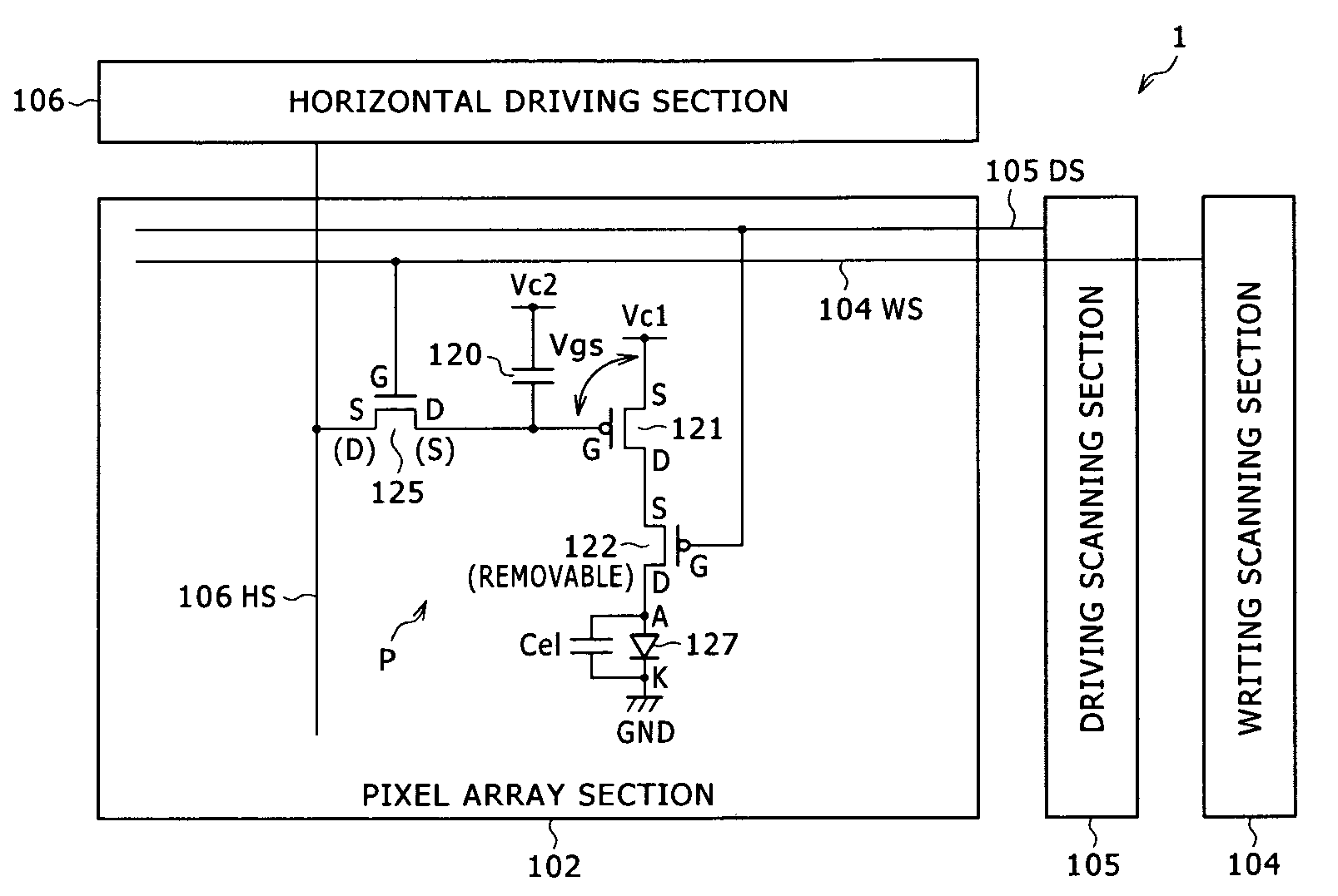
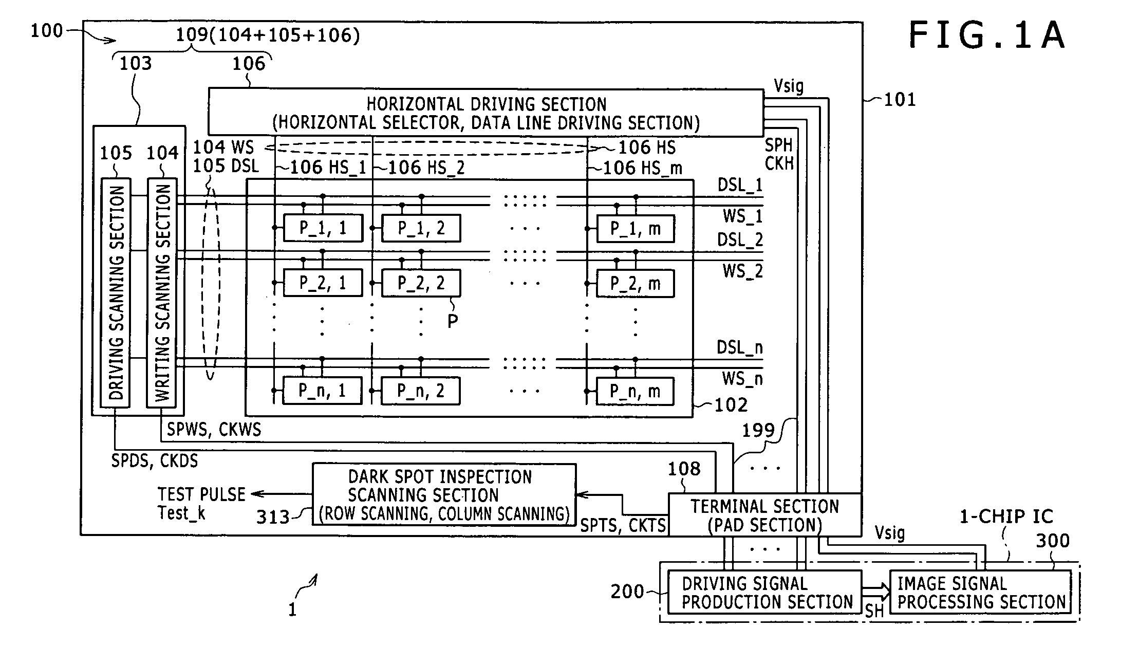
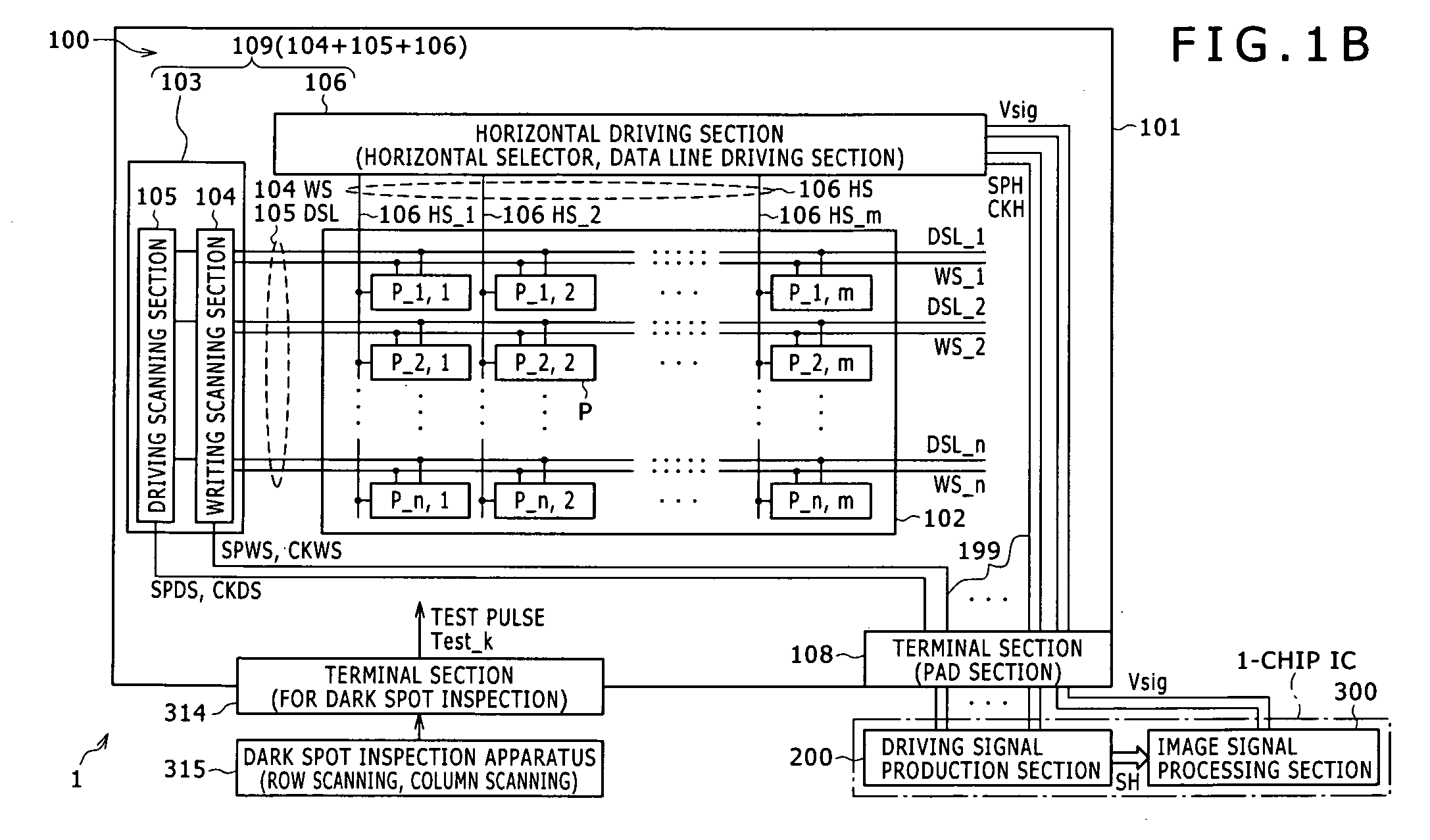
[0083]Referring first to FIGS. 1A and 1B, there are shown different examples of a configuration of an active matrix type display apparatus as a display apparatus according to a preferred embodiment of the present invention. In the present embodiment, the present invention is applied to an active matrix type organic EL display apparatus (hereinafter referred to simply as “organic EL display apparatus”) wherein, for example, an organic EL element and a polysilicon thin film transistor (TFT) are used as a display element (electro-optical element or light emitting element) and an active element of each pixel, respectively. Further, in the organic EL display apparatus, such organic EL elements are formed on a semiconductor substrate on which such thin film transistors are formed.

[0084]It is to be noted that, while an organic EL element is described below particularly as...


PUM


Abstract

A pixel array section includes a plurality of pixel circuits disposed in a matrix and each including a driving transistor, a storage capacitor, an electro-optical element, and a sampling transistor. Each pixel circuit includes a pixel divided into a plurality of divisional pixels for each of which an electro-optical element is provided, and a test transistor provided between the driving transistor and the electro-optical elements for carrying out on/off operations for specifying whether or not the electro-optical element is a dark spot element so that the electro-optical element of the dark spot can be specified. The number of the test transistors is smaller than the number of the divisional elements of the original one pixel.

Description

CROSS REFERENCES TO RELATED APPLICATIONS[0001]The present invention contains subject matter related to Japanese Patent Application JP 2007-307860, filed in the Japan Patent Office on Nov. 28, 2007, the entire contents of which being incorporated herein by reference.BACKGROUND OF THE INVENTION[0002]1. Field of the Invention[0003]This invention relates to a display apparatus which includes a pixel array section including a plurality of pixel circuits (hereinafter referred to also as pixels) disposed in rows and columns and each including an electro-optical element (hereinafter referred to as display element or light emitting element), and also to a fabrication method and a fabrication apparatus for the display apparatus. More particularly, the present invention relates to a display apparatus of the active matrix type wherein a plurality of pixel circuits each including an electro-optical element whose emission light luminance varies depending upon current flowing therethrough are disp...

Claims


Application Information

Patent Timeline
IPC IPC(8): G09G5/00H01J9/42
CPCG09G3/006G09G3/3233G09G2300/0443G09G2300/0819G09G2300/0842G09G2330/10G09G2310/0262G09G2320/0233G09G2320/043G09G2330/08G09G2300/0861G02F1/136G02F1/13G02F1/133
Inventor UCHINO, KATSUHIDEYAMAMOTO, TETSURO
Owner JOLED INC
Why Eureka
Try Eureka