Semiconductor memory device and method of fabricating the same

Inactive Publication Date: 2009-06-04
SK HYNIX INC
View PDF15 Cites 2 Cited by
  • Summary
  • Abstract
  • Description
  • Claims
  • Application Information

AI Technical Summary

Benefits of technology

[0009]The present invention is directed towards semiconductor memory devices and a method of fabricating the same, in which the surface of a floating gate of the semiconductor memory de

Problems solved by technology

It results in significant low margin and decreased reliability of devices, particularly

Method used


Image

  • Semiconductor memory device and method of fabricating the same
  • Semiconductor memory device and method of fabricating the same
  • Semiconductor memory device and method of fabricating the same

Examples


Embodiment Construction

[0016]Now, a specific embodiment according to the present invention will be described with reference to the accompanying drawings. It should be noted that the present invention is not limited to the disclosed embodiment, and may be implemented in various manners. The embodiment described herein is provided to allow a person having ordinary skill in the art to understand the present invention.

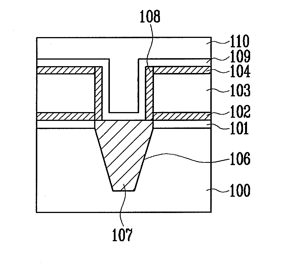
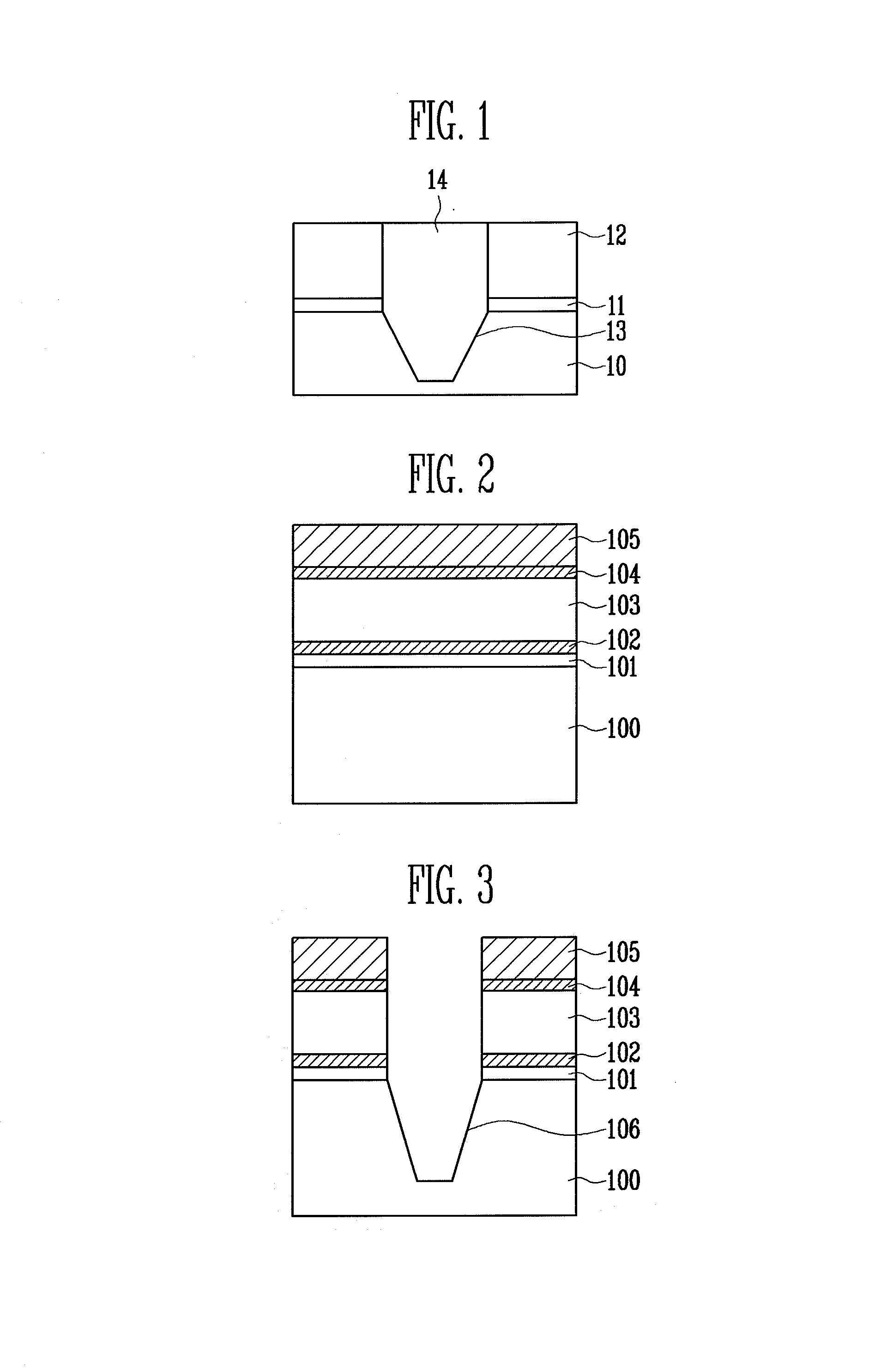
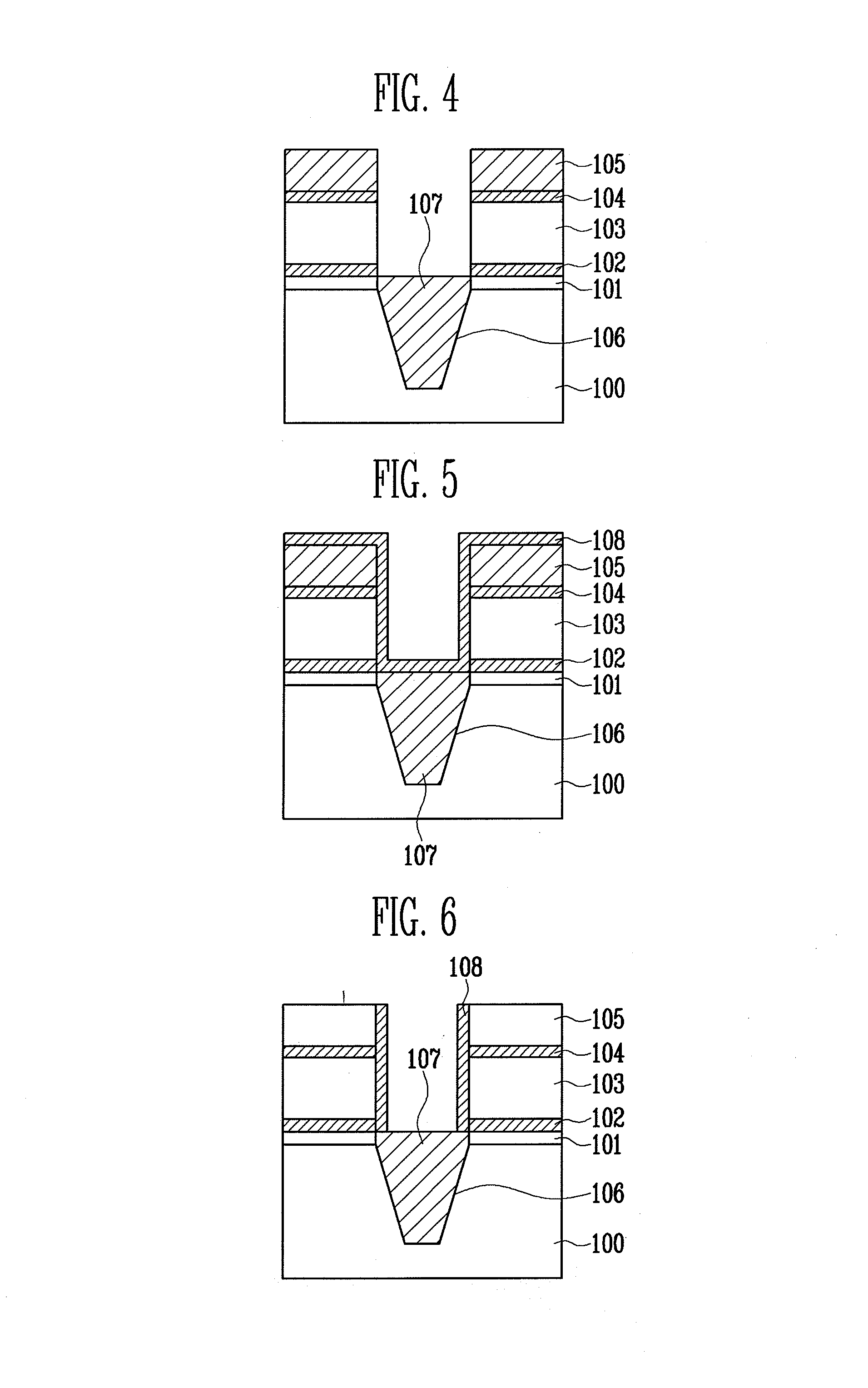
[0017]FIGS. 2 to 7 are sectional views illustrating a method of fabricating a semiconductor memory device in accordance with an embodiment of the present invention.

[0018]Referring to FIG. 2, a tunnel insulating layer 101, a first nano-grain film 102, a conductive layer 103 for a floating gate, a second nano-grain film 104, and a hard mask layer 105 are sequentially formed over a semiconductor substrate 100. The tunnel insulating layer 101 can be formed of an oxide layer. The first and second nano-grain films 102, 104 can be formed by depositing a thin amorphous silicon layer and crystallizing th...


PUM


Abstract

A semiconductor memory devices and a method of fabricating the same includes sequentially stacking a tunnel insulating layer, a first nano-grain film, a conductive layer for a floating gate, and a second nano-grain film over a semiconductor substrate, forming a trench by etching the second nano-grain film, the conductive layer for the floating gate, the first nano-grain film, the tunnel insulating layer, and the semiconductor substrate, gap-filling the trench with an insulating layer, thus forming an isolation layer, and forming a third nano-grain film on sidewalls of the conductive layer for the floating gate.

Description

CROSS-REFERENCES TO RELATED APPLICATIONS[0001]The present application claims priority to Korean patent application number 10-2007-0122617, filed on Nov. 29, 2007, which is incorporated by reference in its entirety.BACKGROUND OF THE INVENTION[0002]The present invention relates to semiconductor memory devices and a method of fabricating the same and, more particularly, to semiconductor memory devices and a method of fabricating the same, in which threshold voltage distributions of semiconductor memory cells can be improved.[0003]A flash memory cell of semiconductor memory devices has a structure in which a tunnel oxide layer, a conductive layer for a floating gate, a dielectric layer, and a conductive layer for a control gate are sequentially stacked over a semiconductor substrate. Program and erase operations of the flash memory cell are performed by injecting or draining electrons into or from the conductive layer for the floating gate.[0004]FIG. 1 is a sectional view illustrating a...

Claims


Application Information

Patent Timeline
IPC IPC(8): H01L29/788H01L21/336
CPCH01L27/115H01L29/7881H01L29/51H01L27/11521H10B69/00H10B41/30B82Y10/00H01L21/76229
Inventor OH, SANG HYUN
Owner SK HYNIX INC
Why Eureka
Try Eureka