Multi-chip stack structure and method for fabricating the same

a stack structure and stack technology, applied in the direction of semiconductor devices, semiconductor/solid-state device details, electrical equipment, etc., can solve the problems of memory chips going out of the packageable range, large package size, high package cost, etc., to avoid wire bonding difficulty and even short circuit problems, reduce the height of the entire structure, and save fabrication costs

Active Publication Date: 2009-06-04
SILICONWARE PRECISION IND CO LTD
View PDF8 Cites 25 Cited by
  • Summary
  • Abstract
  • Description
  • Claims
  • Application Information

AI Technical Summary

Benefits of technology

[0027]Therefore, the present invention comprises disposing a first chip group comprising a plurality of first chips (memory chips) on a chip carrier in a step-like manner; disposing a second chip (a controller chip) on the first chip on top of the first chip group, wherein the first and second chips are electrically connected to the chip carrier through bonding wires; using a film over wire (FOW) technique to stack on the first and second chips a third chip (a memory chip) with an insulative film provided therebetween, wherein the insulative film covers part of the ends of the bonding wires of the first chip on top of the first chip group and at least part of the second chip; and electrically connecting the third chip to the chip carrier through bonding wires. Thus, the controller chip having a size far smaller than the memory chips is prevented from being directly stacked on the memory chips as in the prior art, thereby decreasing height of the entire structure and avoiding wire bonding difficulty and even short ci...

Problems solved by technology

However, the side-by-side structure can lead to a high package cost and large package size since the area of the common substrate needs to increase as the number of the chips increases.
However, if more and more chips are stacked in the above-described way, the projecting area of the entire structure is continuously increased, when a certain number of the stack layers is reached, the memory chips will go out of the packageable range.
Thus, the area of the chip carrier must be increased to finish the chip stack, which however increases the entire package volume and cannot meet requirement of small size and multifunctional electronic products.
Also, as planar size of a controller chip is far smaller than that of a memory chip, when the controller chip is electrically connected to a chip carrier through bonding wires, the bonding wires will definitely pass over the memory chips located below the controller chip, which can easily lead to contact of the bonding wires with the memory chips and ev...

Method used


Image

  • Multi-chip stack structure and method for fabricating the same
  • Multi-chip stack structure and method for fabricating the same
  • Multi-chip stack structure and method for fabricating the same

Examples


first embodiment

[0034]FIGS. 4A to 4D are sectional diagrams showing a multi-chip stack structure and method for fabricating the same according to a first embodiment of the present invention.

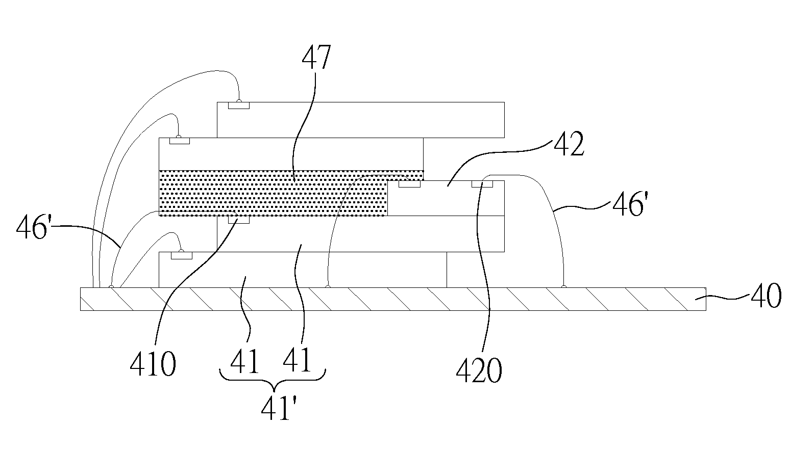
[0035]As shown in FIG. 4A, a chip carrier 40 is provided, a first chip group 41′ comprising a plurality of first chips 41 is disposed on the chip carrier 40 in a step-like manner, and a second chip 42 is disposed on the first chip on the top of the first chip group 41′, wherein the first and second chips 41, 42 are electrically connected to the chip carrier 40 through bonding wires 46.

[0036]The first chips 41 and the second chip 42 can be such as memory chips and a controller chip respectively. Planar size of the second chip 42 is smaller than that of the first chips 41, a plurality of bonding pads 410 is disposed at one side on a surface of each first chip 41 and a plurality of bonding pads 420 is disposed at least one side on a surface of the second chip 42 (the bonding pads 420 are disposed at several sides o...

second embodiment

[0043]FIG. 5 is a diagram showing a multi-chip stack structure and method for fabricating the same according to a second embodiment of the present invention. Different from the first embodiment, the present embodiment electrically connects the first chip on top of the first chip group and the second chip with the chip carrier through a reverse wire bonding method.

[0044]As shown in FIG. 5, a stud bump (not shown) is first formed on the bonding pads 410 of the first chip 41 on top of the first chip group 41′ and the bonding pads 420 of the second chip 42 by a ball bonding method. Then, the bonding wires 46 for electrically connecting the first chip 41 on top of the first chip group 41′, the second chip 42 with the chip carrier 40 have a ball bond formed to connect the chip carrier 40 and have a stitch bond formed to connect the stud bump. Thus, the arc height of the bonding wires electrically connecting the first and second chips 41, 42 with the chip carrier 40 is reduced. Thus, the t...


PUM


Abstract

A multi-chip stack structure and a method for fabricating the same are provided. The method for fabricating a multi-chip stack structure includes disposing a first chip group comprising a plurality of first chips on a chip carrier by using a step-like manner, disposing a second chip on the first chip on top of the first chip group, electrically connecting the first chip group and the second chip to the chip carrier through bonding wires, using film over wire (FOW) to stack a third chip on the first and the second chips with an insulative film provided therebetween, wherein the insulative film covers part of the ends of the bonding wires of the first chip on the top of the first group and at least part of the second chip, and electrically connecting the third chip to the chip carrier through bonding wires, thereby preventing directly disposing on a first chip a second chip having a planar size far smaller than that of the first chip as in the prior art that increases height of the entire structure and increases the wiring bonding difficulty.

Description

BACKGROUND OF THE INVENTION[0001]1. Field of the Invention[0002]The present invention relates generally to a semiconductor structure and method for fabricating the same, and more particularly to a multi-chip stack structure and method for fabricating the same.[0003]2. Description of Related Art[0004]Currently, multi-chip module (MCM) semiconductor packages have been developed to improve performance and capacity of single semiconductor packages, thereby meeting the demand for electronic products having smaller size and higher operation speed. Typically, two or more chips are disposed in a multi-chip module semiconductor package so as to reduce the entire structure volume of electronic products and improve electrical performance of the electronic products. In other words, by combining two or more chips in a single package structure, limit on the system operation speed is minimized, and in addition, the multi-chip package structure can reduce length of connecting circuit between the ch...

Claims


Application Information

Patent Timeline
IPC IPC(8): H01L23/52H01L21/00
CPCH01L23/3107H01L2924/15313H01L25/0657H01L25/18H01L25/50H01L2224/48091H01L2224/48227H01L2224/73265H01L2225/0651H01L2225/06555H01L2225/06562H01L2225/06575H01L2924/01082H01L2924/15311H01L24/32H01L2225/06506H01L2924/1436H01L2924/1438H01L2924/15323H01L2924/15321H01L21/56H01L24/85H01L2224/858H01L2224/83H01L2224/32225H01L2224/32145H01L24/83H01L2924/01033H01L2924/00014H01L2924/00H01L2924/00012H01L24/73H01L2924/181H01L2224/05554H01L24/48H01L2224/8592H01L2224/45099H01L2224/05599
Inventor LIU, CHUNG-LUNHUANG, JUNG-PINCHANG, YI-FENGCHANG, CHIN-HUANG
Owner SILICONWARE PRECISION IND CO LTD
Why Eureka
Try Eureka