
Magnetic Random Access Memory

a random access and magnetic technology, applied in the field of magnetic random access memory, can solve the problems of operation instability and the possibility of write disturbance, and achieve the effect of enlarger the write operation region and suppressing the disturban

Active Publication Date: 2009-06-04
NEC CORP
View PDF8 Cites 23 Cited by
  • Summary
  • Abstract
  • Description
  • Claims
  • Application Information

AI Technical Summary

Benefits of technology

[0034]The object of the present invention is to provide an MRAM employing an SAF structure that can suppress disturbance and can enlarge a write operation region.
[0035]Another object of the present invention is to provide an MRAM employing an SAF structure that can suppress disturbance and can reduce a write current.
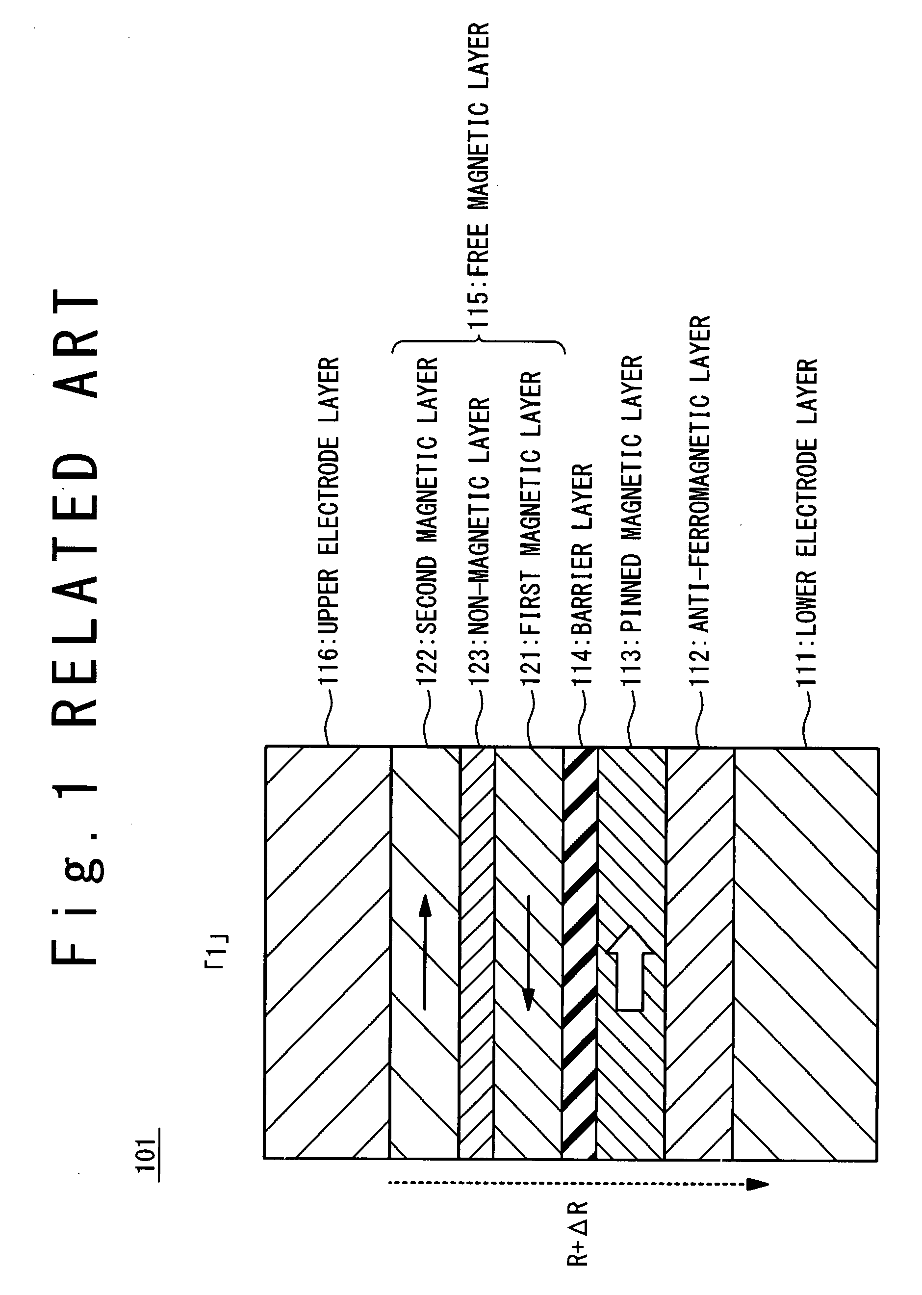
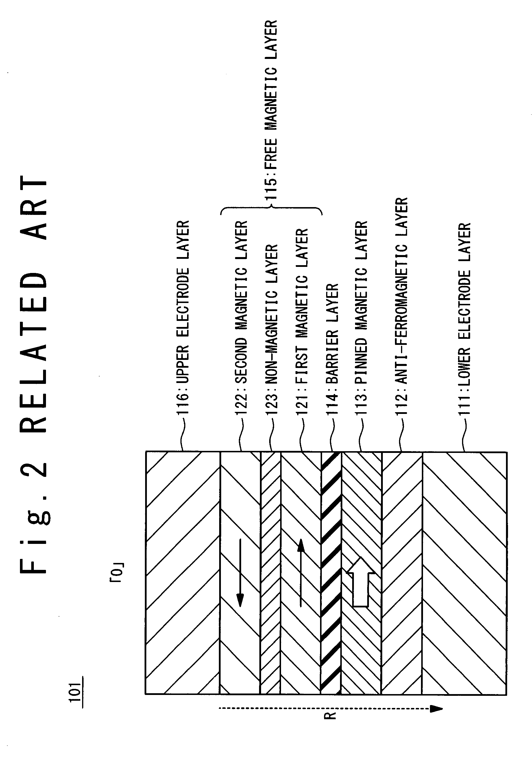
[0037]Here, the magnetic random access memory (MRAM) contains a plurality of first wirings, a plurality of second wirings and a plurality of memory cells. The plurality of first wirings extend in a first direction. The plurality of second wirings extend in a second direction substantially orthogonal to the first direction. The plurality of memory cells include a free magnetic layers in which a plurality of magnetic layers coupled through non-magnetic layers anti-ferromagnetically are laminated, and they are provided for the respective points at which the plurality of first wirings and the plurality of second wirings intersect. The direction of a magnetization easy axis of the free magnetic layer is different between the first direction and the second direction. The writing method contains: (a) reading a first data stored in a selection cell selected from the plurality of memory cells; (b) comparing a second data to be written to the selection cell and the first data; and (c) supplying a first write current to a selection first wiring corresponding to the selection cell among the plurality of first wirings, in the direction based on the second data, and supplying a second write current to a selection second wiring corresponding to the selection cell among the plurality of second wirings, in the direction based on the second data. In the MRAM of the present invention, irrespectively of the relation of the spontaneous magnetizations and film thicknesses between the respective magnetic layers in the free magnetic layer, a write operation can be performed in any of a toggle write region and a direct write region. That is, the operation region can be enlarged. In addition, the direct write region can be used to reduce the write current. That is, the electric power consumption can be decreased. Also, since the write current can be reduced, the area of the transistors related to the write current can be decreased. That is, the chip area of the MRAM can be made relatively small, or the region of the memory cell can be made relatively wide.
[0039]In the writing method of the magnetic random access memory, the free magnetic layer has two layers of a first magnetic film and a second magnetic film, and a spontaneous magnetization M1 and a film thickness t1 of the first magnetic film and a spontaneous magnetization M2 and a film thickness t2 of the second magnetic film satisfy M1×t1≠M2×t2. In the present invention, the product of the spontaneous magnetization and the film thickness is not required to be set equal between the magnetic films. Thus, the manufacturing margin of the magnetic film can be set wide. That is, the manufacturing yield of the MRAM can be made high.
[0043]In the writing method of the magnetic random access memory, the free magnetic layer includes magnetic layers of one of (2n+1) layers (n: an integer of 1 or more) and 2n layers, and a spontaneous magnetization Ms2p-1 and a film thickness t2p-1 of the magnetic layer of a (2p−1)-th layer and a spontaneous magnetization Ms2p and a film thickness t2p of the magnetic layer of a 2p-th layer satisfy the following equation, by setting q=n+1 in case of the (2n+1) layers and q=n in case of the 2n layers:∑p=1q(Ms2p-1×t2p-1)≠∑p=1q(Ms2p×t2p)In the present invention, since the product of the spontaneous magnetization and the film thickness is not required to be equal between the magnetic films, the manufacturing margin of the magnetic film can be set wide. That is, the manufacturing yield of the MRAM can be made high.

Problems solved by technology

As a result, the possibility of the write disturbance becomes higher.
At this time, the operation becomes unstable.

Method used


Image

  • Magnetic Random Access Memory
  • Magnetic Random Access Memory
  • Magnetic Random Access Memory

Examples


first example

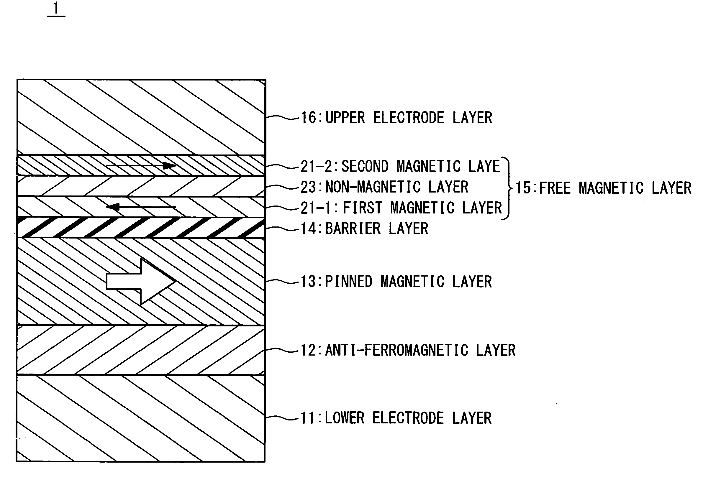
[0145]FIG. 23 is a sectional view showing a magnetic resistance element having a structure A. This magnetic resistance element contains a seed layer 17, an anti-ferromagnetic layer 12, a fixed magnetic layer 13, a barrier layer 14, a free magnetic layer 15 and a cap layer 18, which are laminated in turn on the substrate. The seed layer 17 is a Ta film having the film thickness of 20 nm. The anti-ferromagnetic layer 12 is a PtMn film having the film thickness of 20 nm. The fixed magnetic layer 13 is composed of a CoFe film having the film thickness of 2.5 nm, a Ru film having the film thickness of 0.88 nm and a CoFe film having the film thickness of 2.5 nm. The barrier layer 14 is a film in which an Al film having the film thickness of 1 nm is oxidized. The free magnetic layer 15 has the magnetic films of alternately laminated two layers and one non-magnetic film. The first magnetic film 21-1 is composed of a NiFe film having the film thickness of 4 nm and a CoFe film having the film...

second example

[0153]FIG. 27 is a sectional view showing the magnetic resistance element having the structure B. This magnetic resistance element contains a seed layer 17, an anti-ferromagnetic layer 12, a fixed magnetic layer 13, a barrier layer 14, a free magnetic layer 15 and a cap layer 18, which are laminated in turn on the substrate. The seed layer 17 is a Ta film having the film thickness of 20 nm. The anti-ferromagnetic layer 12 is a PtMn film having the film thickness of 20 nm. The fixed magnetic layer 13 is composed of a CoFe film having the film thickness of 2.5 nm, a Ru film having the film thickness of 0.88 nm and a CoFe film having the film thickness of 2.5 nm. The barrier layer 14 is a film in which an Al film having the film thickness of 1 nm is oxidized. The free magnetic layer 15 has the magnetic films of the alternately laminated two layers and the non-magnetic film. The first magnetic film 21-1 is composed of a Co75Fe25 film having the film thickness of 2 nm and a CoFeB film ha...

third example

[0161]FIG. 31 is a sectional view showing the magnetic resistance element having the structure C. This magnetic resistance element contains a seed layer 17, a anti-ferromagnetic layer 12, a fixed magnetic layer 13, a barrier layer 14, a free magnetic layer 15 and a cap layer 18, which are laminated in turn on the substrate. The seed layer 17 is a Ta film having the film thickness of 20 nm. The anti-ferromagnetic layer 12 is a PtMn film having the film thickness of 20 nm. The fixed magnetic layer 13 is composed of a CoFe film having the film thickness of 2.5 nm, a Ru film having the film thickness of 0.88 nm and a CoFe film having the film thickness of 2.5 nm. The barrier layer 14 is a film in which an Al film having the film thickness of 1 nm is oxidized. The free magnetic layer 15 has magnetic films of the alternately laminated two layers and the non-magnetic film. The first magnetic film 21-1 is composed of a CoFeB film having the film thickness of 3.1 nm and a CoFe film having th...


PUM


Abstract

MRAM includes a first wiring, a second wiring, and a memory cell. The first wiring extends to a first direction, and the second wiring extends to a second direction. The memory cell includes a free magnetic layer in which a plurality of magnetic layers coupled anti-ferromagnetically through non-magnetic layers are laminated, and is provided at an intersection of the first and second wirings. The magnetization direction of the free magnetic layer is different from the first and second directions. The writing method includes (a) reading a first data stored in the memory cell; (b) comparing a second data to be written to the memory cell and the first data; and (c) changing a direction of a first write current supplied to the first wiring and a direction of the second write current to be supplied to the second wiring, when the first data and second data are different.

Description

TECHNICAL FIELD[0001]The present invention relates to a magnetic random access memory (MRAM), and more particularly relates to a magnetic random access memory having a lamination ferry structure.BACKGROUND ART[0002]The magnetic random access memory (MRAM) is a hopeful non-volatile memory from the viewpoint of high integration and high speed operation. In the MRAM, a magnetic resistance element is used which shows a magnetic resistance effect such as an AMR (Anisotropic Magneto Resistance) effect, a GMR (Giant Magneto Resistance) effect and a TMR (Tunnel Magneto Resistance) effect.[0003]U.S. Pat. No. 5,640,343 discloses a typical MRAM. In this MRAM, in such a way that an erroneous write (write disturbance) to a half-selection cell does not occur at a time of a write operation, the value of a write current is limited to a predetermined write margin. However, in the magnetic resistance element of each memory cell in the MRAM, a variation exists in its characteristic. As the variation i...

Claims


Application Information

Patent Timeline
IPC IPC(8): G11C11/02G11C11/14G11C11/416
CPCH01L43/08G11C11/16G11C11/1659G11C11/161G11C11/1675G11C11/1657H10N50/10
Inventor MIURA, SADAHIKOSUGIBAYASHI, TADAHIKOSUZUKI, TETSUHIRO
Owner NEC CORP
Learn More