Solar Cell Contact Formation Process Using A Patterned Etchant Material

a solar cell and patterned technology, applied in the direction of basic electric elements, electrical equipment, semiconductor devices, etc., can solve the problems of prior manufacturing methods and the cost of solar cell completion, and achieve the effect of improving the efficiency of solar cell production

Inactive Publication Date: 2009-06-04
APPLIED MATERIALS INC
View PDF92 Cites 79 Cited by
  • Summary
  • Abstract
  • Description
  • Claims
  • Application Information

AI Technical Summary

Benefits of technology

[0009]The present invention also provides a method of forming a method of forming a solar cell device, comprising forming a dielectric layer on at least one surface of a substrate, wherein the dielectric layer contains one or more doping elements, disposing an etchant material on a plurality of regions of the dielectric layer, wherein the etchant material comprises ammonium fluoride, heating the substrate to a desired temperature to causes the etchant material to remove at least a portion of the dielectric layer, and depositing a conducting layer on the silicon containing region.

Problems solved by technology

However, there are several issues with these prior manufacturing methods.
For example, the formation processes are complicated multistep processes that add to costs required to complete the solar cells.

Method used


Image

  • Solar Cell Contact Formation Process Using A Patterned Etchant Material
  • Solar Cell Contact Formation Process Using A Patterned Etchant Material
  • Solar Cell Contact Formation Process Using A Patterned Etchant Material

Examples


Embodiment Construction

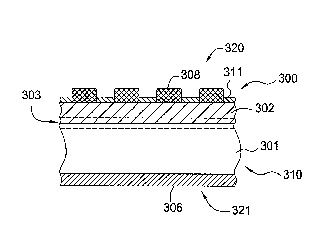
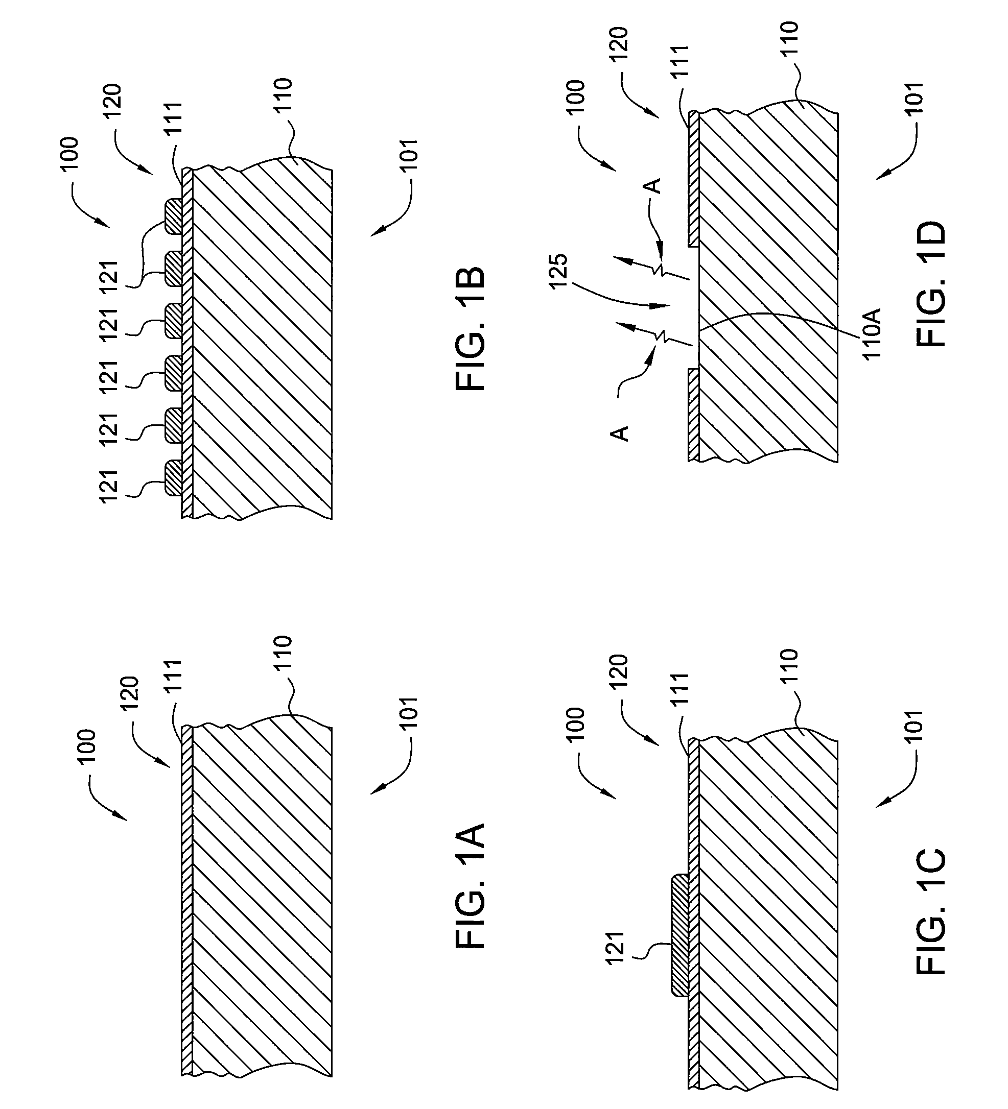
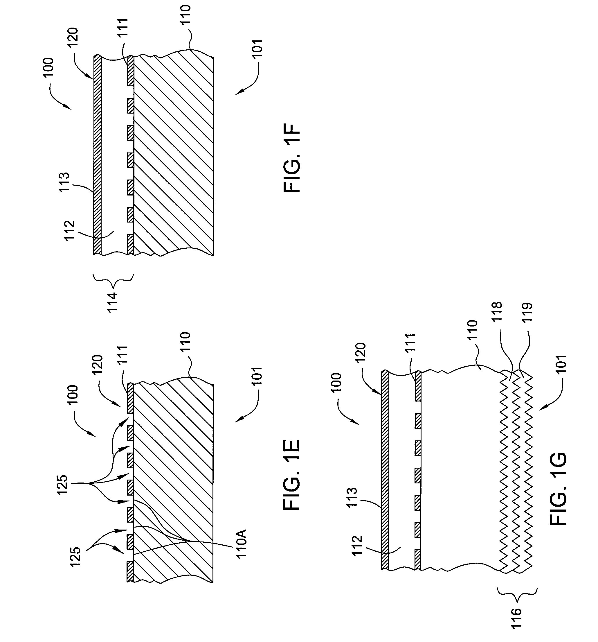
[0018]Embodiments of the invention contemplate the formation of a high efficiency solar cell using novel methods to form the active region(s) and the metal contact structure of a solar cell device. In one embodiment, the methods include the use of various etching and patterning processes that are used to define point contacts through a blanket dielectric layer covering a surface of a solar cell substrate. The method generally includes depositing an etchant material that enables formation of a desired pattern in a dielectric layer through which electrical contacts to the solar cell device can be formed. Various techniques may be used to form the active regions of the solar cell and the metal contact structure. Solar cell substrates (e.g., substrate 110 in FIG. 1A) that may benefit from the invention include flexible substrates that may have an active region that contains organic material, single crystal silicon, multi-crystalline silicon, polycrystalline silicon, germanium (Ge), gall...


PUM


Abstract

Embodiments of the invention contemplate the formation of a high efficiency solar cell using novel methods to form the active region(s) and the metal contact structure of a solar cell device. In one embodiment, the methods include the use of various etching and patterning processes that are used to define point contacts through a blanket dielectric layer covering a surface of a solar cell substrate. The method generally includes depositing an etchant material that enables formation of a desired pattern in a dielectric layer through which electrical contacts to the solar cell device can be formed.

Description

CROSS-REFERENCE TO RELATED APPLICATIONS[0001]This application claims benefit of U.S. Provisional Patent Application Ser. No. 61 / 003,754 [Attorney Docket # APPM 12974L], filed Nov. 19, 2007, U.S. Provisional Patent Application Ser. No. 61 / 048,001 [Attorney Docket # APPM 13439L], filed Apr. 25, 2008, and U.S. Provisional Patent Application Ser. No. 61 / 092,379 [Attorney Docket # APPM 13437L], filed Aug. 27, 2008, which are all herein incorporated by reference.BACKGROUND OF THE INVENTION[0002]1. Field of the Invention[0003]Embodiments of the invention generally relate to the fabrication of photovoltaic cells.[0004]2. Description of the Related Art[0005]Solar cells are photovoltaic devices that convert sunlight directly into electrical power. The most common solar cell material is silicon, which is in the form of single or multicrystalline substrates, sometimes referred to as wafers. Because the amortized cost of forming silicon-based solar cells to generate electricity is higher than th...

Claims


Application Information

Patent Timeline
Patent Type & Authority Applications(United States)
IPC IPC(8): H01L21/02H01L31/18
CPCY02E10/50H01L31/022425
Inventor WEIDMAN, TIMOTHY W.MISHRA, ROHIT
Owner APPLIED MATERIALS INC
Why Eureka
Try Eureka