Electronic component mounting package

Active Publication Date: 2009-06-11
SHINKO ELECTRIC IND CO LTD
View PDF10 Cites 57 Cited by
  • Summary
  • Abstract
  • Description
  • Claims
  • Application Information

AI Technical Summary

Benefits of technology

[0014]An object of the present invention is to provide an electronic component mounting package which are capable of effectively reducing warpage in a substrate that can possibly occur at the time of packaging of an electronic component such as a semiconductor device or at other times, thereby contributing to highly-reliable mounting.
[0016]In the configuration of the electronic component mounting package according to the present invention, the entire surface of the structure (wiring board) is covered with the molding resin, exclusive of a predetermined portion (i.e., the pad portion to which an external terminal is to be connected) of the structure in which the wiring and insulating layers are alternatingly stacked one on top of another. Thereby, the rigidity of the overall substrate is improved. Therefore, the covering of the molding resin provides reinforcement of the overall substrate, and thus enables effective prevention of propagation of a stress, if any, through the substrate, the stress (namely, the stress that can possibly cause warpage in the substrate) induced according to the difference in the coefficient of thermal expansion between the package and an electronic component at the interface therebetween when the electronic component is mounted on the package using a thermosetting material.
[0017]This enables an effective reduction in the warpage in the overall substrate, thus eliminating a disadvantage of chip “delamination,” such as encountered in the prior art, and thereby enabling highly-reliable chip mounting of the electric component.
[0018]Also, the electronic component mounting package according to the above-described aspect may further include an interposer mounted on the side of the electronic component mounting surface and connected to the pad portion, and the molding resin may be partially filled into a gap between the structure and the interposer. In this configuration, the presence of the interposer enables an effective reduction in the influence (namely, the warpage in the substrate) resulting from the difference in the coefficient of thermal expansion when the electronic component is mounted on the wiring board. Also, this configuration makes it possible for the wiring board to enable high-density packaging based on the essential function of the interposer.
[0020]In the configuration of the electronic component mounting package according to this aspect, as distinct from the electronic component mounting package according to the above-described aspect, the structure itself is not covered directly with the molding resin; however, the entire surface of the wiring board with the structure fixedly mounted thereon is covered with the molding resin. Thereby, the rigidity of the overall package inclusive of the structure can be improved. This enables an effective reduction in the warpage in the overall substrate, thus enabling highly-reliable chip mounting of the electronic component, as in the case of the package according to the above-described aspect.

Problems solved by technology

This leads to a limitation to making the entire package thinner.
On the other hand, the conventional coreless substrate has a disadvantage of being prone to “warpage” since the absence of the core substrate affords the overall package low rigidity.
This problem develops more markedly when a chip is mounted on the substrate.
However, this causes a shrinkage in the underfill resin and in turn leads to warpage in the periphery of the substrate toward the chip mounting surface, due to the fact that the coefficient of thermal expansion of the chip is different from that of the substrate.
Thus, in the structure of the conventional coreless substrate (semiconductor package), the low rigidity of the overall package causes a “warpage” during chip mounting, and this can possibly cause chip delamination, depending on the degree of warpage.
Accordingly, the structure has a problem in that reliable chip mounting is impossible with the structure.
Additionally, the timing of the warpage to occur in the substrate is not limited to only the time of chip mounting, but also the warpage may possibly occur even at stages before chip mounting.
For example, in the case where a coreless substrate is delivered and then a chip is mounted thereon, the warpage can possibly occur in the substrate, depending on how the substrate is handled during the processes from the delivery to the mounting, because the coreless substrate is intrinsically low in rigidity and flexible.
Moreover, this problem is not necessarily unique to the coreless substrate and may possibly likewise arise in a build-up multilayer wiring board having the core substrate.
As a result, the warpage may occur in the substrate.

Method used


Image

  • Electronic component mounting package
  • Electronic component mounting package
  • Electronic component mounting package

Examples


first embodiment

. . . See FIGS. 1 and 2

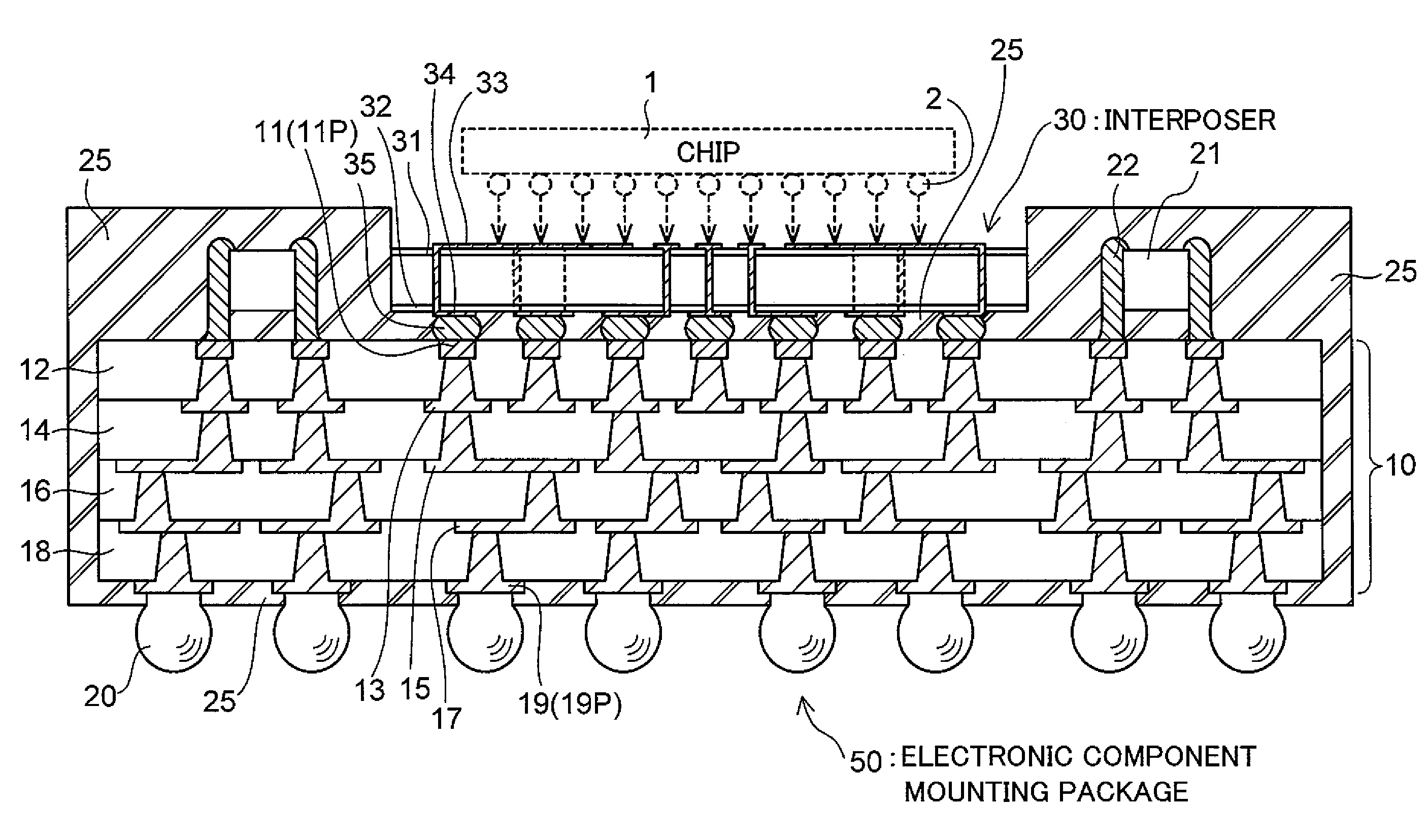
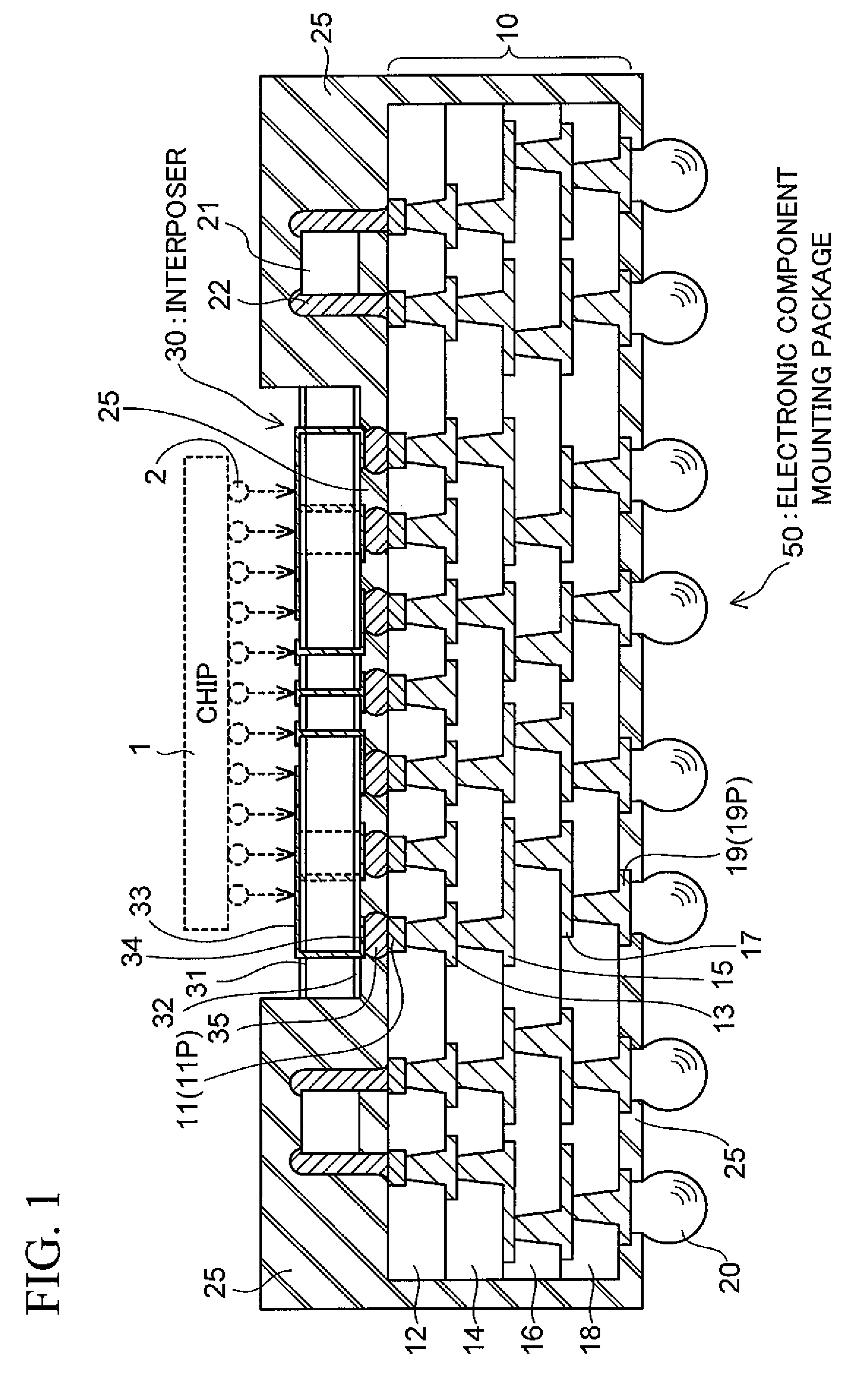
[0027]FIG. 1 shows, in a sectional form, the configuration of an electronic component mounting package according to a first embodiment of the present invention.

[0028]The electronic component mounting package 50 according to this embodiment basically includes: a wiring board (coreless substrate) 10 that does not contain a support base member; and an interposer 30 mounted on the coreless substrate 10. The package 50 according to this embodiment is provided with a chip (typically, a silicon (Si) chip) 1, such as a semiconductor device, mounted on the interposer 30 as shown by the dashed line in FIG. 1, with the interposer 30 mounted on the coreless substrate 10 as shown in FIG. 1. Thereby, the package 50 forms an electronic component device for a semiconductor device or the like.

[0029]As shown in FIG. 1, the coreless substrate 10 that constitutes a principal part of the package 50 has a structure in which a plurality of wiring layers 11, 13, 15, 17 and 19 are sta...

second embodiment

. . . See FIGS. 3 and 4

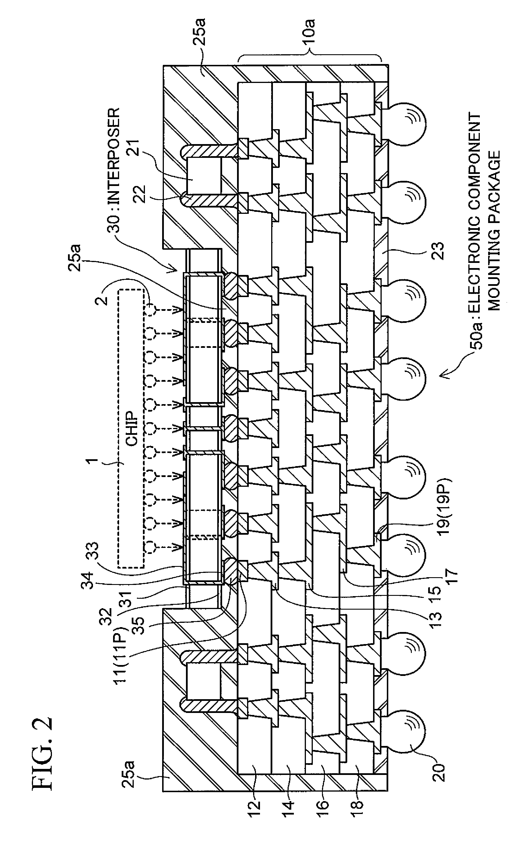
[0053]With the configurations of the electronic component mounting packages 50 and 50a according to the above-mentioned first embodiment and the modified example thereof (see FIGS. 1 and 2), description is given taking the case where the coreless substrates 10 and 10a are directly covered with the molding resins 25 and 25a, respectively, to thereby provide reinforcement to the substrates and thus reduce the warpage therein. Of course, however, the object to be covered with the molding resin is not necessarily limited to any one of the coreless substrates 10 and 10a, as is also apparent from the gist of the present invention. It is essential only that the covering with the molding resin permits an improvement in the rigidity of the overall package. Description is given below with respect to an embodiment in this case.

[0054]FIG. 3 shows, in sectional form, the configuration of an electronic component mounting package according to a second embodiment of the prese...


PUM


Abstract

An electronic component mounting package includes a structure (coreless substrate) in which a plurality of wiring layers are stacked one on top of another with insulating layers interposed therebetween and are interconnected through via holes formed in the insulating layers. The entire surface of the coreless substrate, exclusive of pad portions defined at desired positions of the outermost wiring layers thereof, is covered with a molding resin. Further, an interposer is mounted on the side of the electronic component mounting surface of the coreless substrate, and the molding resin is partially filled into a gap between the coreless substrate and the interposer.

Description

CROSS-REFERENCE TO RELATED APPLICATIONS[0001]This application is based on and claims priority of Japanese Patent Application No. 2007-314280 filed on Dec. 5, 2007, the entire contents of which are incorporated herein by reference.BACKGROUND OF THE INVENTION[0002](a) Field of the Invention[0003]The present invention relates to a wiring board for use in mounting an electronic component such as a semiconductor device. More particularly, the present invention relates to a wiring board (hereinafter referred to as an “electronic component mounting package” or merely as a “package”) adapted for mounting an electronic component using a thermosetting material, the wiring board having a structure of a multilayer wiring board in which a plurality of wiring layers are stacked one on top of another with an insulating layer interposed therebetween and are interconnected through via holes formed in the insulating layer.[0004](b) Description of the Related Art[0005]Conventionally, build-up process ...

Claims


Application Information

Patent Timeline
IPC IPC(8): H01R12/02H01R12/50
CPCH01L21/6835H01L2224/16235H01L23/315H01L23/49816H01L23/49822H01L23/49827H01L24/16H01L2221/68345H01L2924/0102H01L2924/01078H01L2924/01079H01L2924/09701H01L2924/15311H01L2924/19041H01L2924/19105H01L2924/3025H05K3/284H05K3/3436H05K2201/0989H05K2201/10378H05K2201/10734H05K2201/10977H01L2224/16225H01L2924/10253H01L23/3128H01L2924/00
Inventor MIKI, SYOTAARAI, TADASHI
Owner SHINKO ELECTRIC IND CO LTD
Why Eureka
Try Eureka