Nitride semiconductor device

Active Publication Date: 2009-06-11
SAMSUNG ELECTRONICS CO LTD
View PDF8 Cites 4 Cited by
  • Summary
  • Abstract
  • Description
  • Claims
  • Application Information

AI Technical Summary

Benefits of technology

[0018]An aspect of the present invention provides a nitride semiconductor device significantly improved i

Problems solved by technology

Also, carriers are limitedly injected to a specific local area of the active layer to thereby reduce an effective active area i

Method used


Image

  • Nitride semiconductor device
  • Nitride semiconductor device
  • Nitride semiconductor device

Examples


Embodiment Construction

[0041]Exemplary embodiments of the present invention will now be described in detail with reference to the accompanying drawings. This invention may, however, be embodied in many different forms and should not be construed as limited to the embodiments set forth herein. Rather, these embodiments are provided so that this disclosure will be thorough and complete, and will fully convey the scope of the invention to those skilled in the art. In the drawings, the shapes and dimensions may be exaggerated for clarity, and the same reference signs are used to designate the same or similar components throughout.

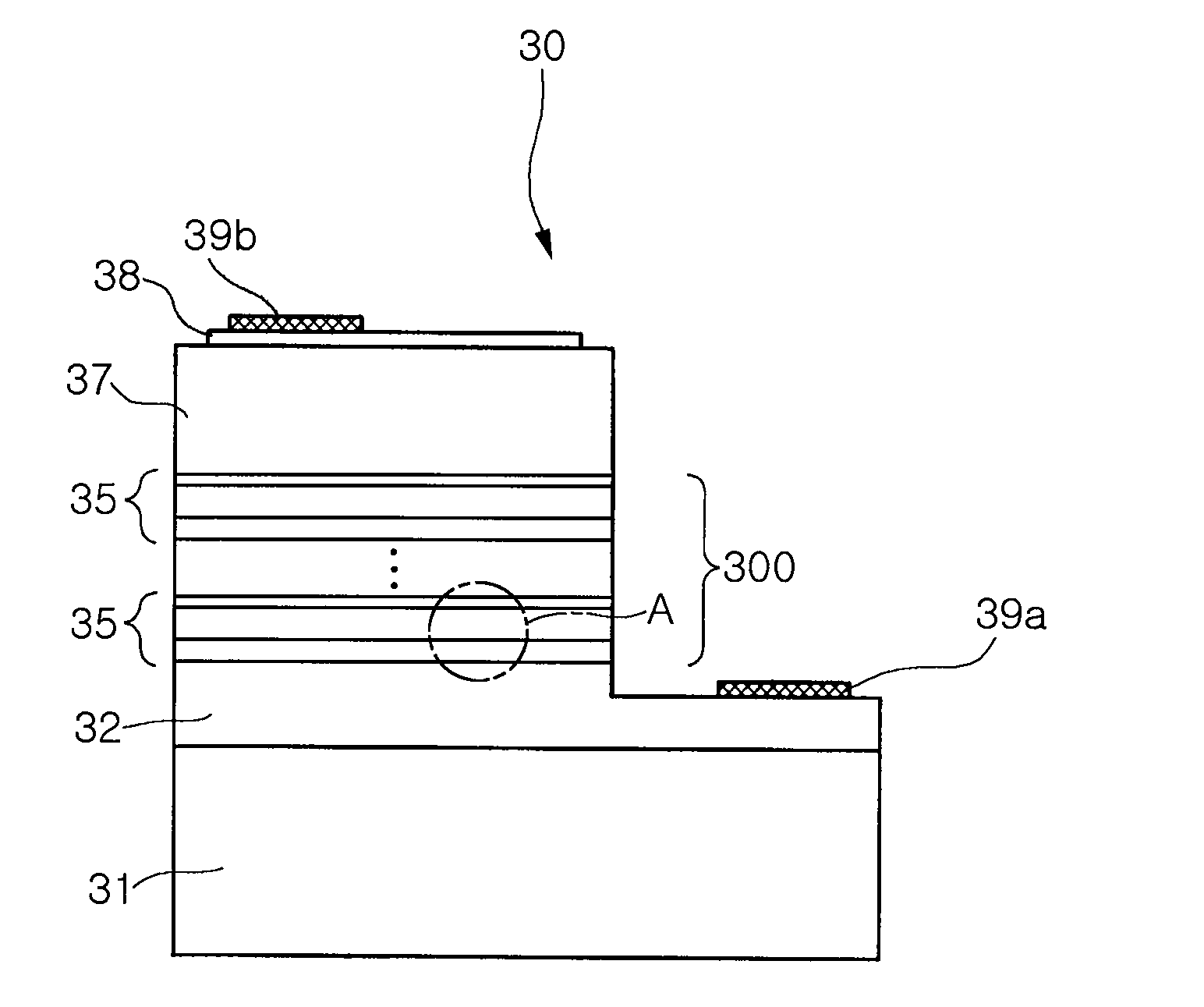
[0042]FIG. 3 is a cross-sectional view illustrating a nitride semiconductor device according to an exemplary embodiment of the invention. FIG. 4 is a magnified view illustrating an area indicated with A in FIG. 3.

[0043]First, referring to FIG. 3, the nitride semiconductor device 30 includes a substrate 31, an n-type nitride semiconductor layer 32, an active layer 300 and a p-type nit...


PUM


Abstract

There is provided a nitride semiconductor device including: an n-type nitride semiconductor layer; a p-type nitride semiconductor layer; and an active layer formed between the n-type and p-type nitride semiconductor layers, the active layer including a plurality of quantum well layers and at least one quantum barrier layer deposited alternately with each other, wherein the active layer includes a first quantum well layer, a second quantum well layer formed adjacent to the first quantum well layer toward the p-type nitride semiconductor layer and having a quantum level higher than a quantum level of the first quantum well layer, and a tunneling quantum barrier layer formed between the first and second quantum well layers and having a thickness enabling a carrier to be tunneled therethrough.

Description

CROSS-REFERENCE TO RELATED APPLICATIONS[0001]This application claims the priority of Korean Patent Application No. 2007-0126131 filed on Dec. 6, 2007, in the Korean Intellectual Property Office, the disclosure of which is incorporated herein by reference.BACKGROUND OF THE INVENTION[0002]1. Field of the Invention[0003]The present invention relates to a nitride semiconductor device, and more particularly, to a nitride semiconductor device improved in emission efficiency due to an active layer having an optimal structure of quantum barrier and quantum well layers, notably, when operating in a high current.[0004]2. Description of the Related Art[0005]In general, a nitride semiconductor is broadly utilized in a green or blue light emitting diode (LED) or a laser diode (LD) which serves as a light source in a full color display, an image scanner, various signal systems and optical communication devices. This nitride semiconductor device may act as a light emitting device including an acti...

Claims


Application Information

Patent Timeline
IPC IPC(8): H01L33/00H01L33/06H01L33/32
CPCH01L33/06B82Y20/00B82Y10/00H01L33/32
Inventor LEE, SOO MINPARK, HEE SEOKHAN, JAE WOONGLEE, SEONG SUKSONE, CHEOL SOO
Owner SAMSUNG ELECTRONICS CO LTD
Why Eureka
Try Eureka