Structure and method to increase effective mosfet width

a technology of effective mosfet and structure, which is applied in the direction of semiconductor devices, electrical equipment, basic electric elements, etc., can solve the problems of reducing drive capability, affecting performance and circuit stability, and difficult to fill the sti, so as to achieve the effect of increasing the effective device width

Inactive Publication Date: 2009-06-11
ALSEPHINA INNOVATIONS INC
View PDF8 Cites 14 Cited by
  • Summary
  • Abstract
  • Description
  • Claims
  • Application Information

AI Technical Summary

Benefits of technology

[0023]According to the invention, generally, the effective width of an active silicon region (RX) bordered by STI is increased by disposing an epitaxial silicon layer on the substrate, overhanging the trench. Lateral growth of the epitaxial layer may be facilitated when the RX has <100> crystal orientation.
[0025]In this manner, the effective device width can be increased, while keeping the same RX pitch, STI width and same well isolation.
[0032]Effective W of the device is increased, therefore performance may be improved with same density.

Problems solved by technology

As the width is scaled down, the drive capability is reduced and it will affect the performance and circuit stability.
But it will make it very difficult to fill the STI and also keep good isolation.

Method used


Image

  • Structure and method to increase effective mosfet width
  • Structure and method to increase effective mosfet width
  • Structure and method to increase effective mosfet width

Examples


Embodiment Construction

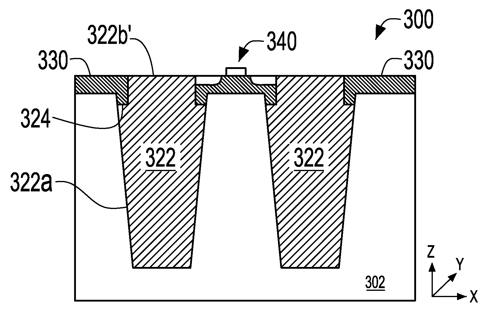
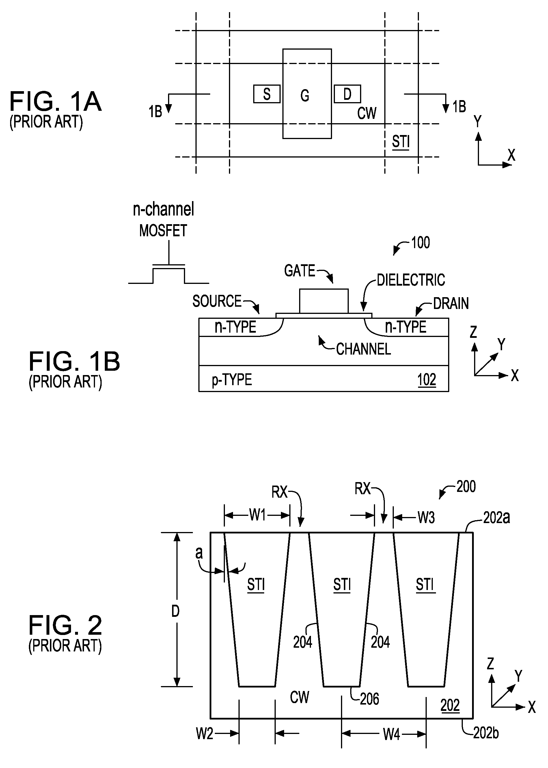
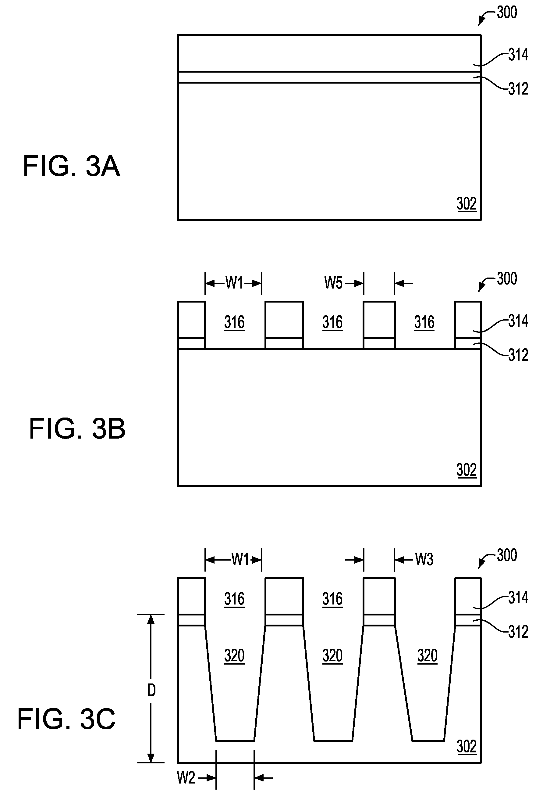
[0045]In the description that follows, numerous details are set forth in order to provide a thorough understanding of the present invention. It will be appreciated by those skilled in the art that variations of these specific details are possible while still achieving the results of the present invention. Well-known processing steps are generally not described in detail in order to avoid unnecessarily obfuscating the description of the present invention.

[0046]Throughout the descriptions set forth in this disclosure, lowercase numbers or letters may be used, instead of subscripts. For example Vg could be written Vg. Generally, lowercase is preferred to maintain uniform font size.) Regarding the use of subscripts (in the drawings, as well as throughout the text of this document), sometimes a character (letter or numeral) is written as a subscript—smaller, and lower than the character (typically a letter) preceding it, such as “Vs” (source voltage) or “H2O” (water). For consistency of ...


PUM


Abstract

An epitaxial layer of silicon (Si) or silicon-germanium (SiGe) extends over the edge of silicon trench isolation (STI), thereby increasing the effective width of an active silicon region (RX) bordered by the STI. The RX region may have a <100> crystal orientation. An effective width of an FET device formed in the RX region may be increased, therefore performance may be improved with same density. Isolation may not be degraded since RX-to-RX distance is same at bottom. Junction capacitance may be reduced since part of the RX is on STI.

Description

FIELD OF THE INVENTION[0001]The invention relates to the manufacture of semiconductor devices and, more particularly, field effect transistors (FETs) and, more particularly, to trench-isolated FETs.BACKGROUND OF THE INVENTION[0002]U.S. Pat. No. 5,643,822 (IBM, 1997), incorporated by reference in its entirety herein, discloses a method for forming trench-isolated field effect transistor (FET) devices.[0003]The transistor is a solid state semiconductor device which can be used for amplification, switching, voltage stabilization, signal modulation and many other functions. Generally, a transistor has three terminals, and a voltage applied to a specific one of the terminals controls current flowing between the other two terminals.[0004]The terminals of a field effect transistor (FET) are commonly named source, gate and drain. In the FET, a small amount of voltage is applied to the gate (G) in order to control current flowing between the source (S) and drain (D). In FETs, the main curren...

Claims


Application Information

Patent Timeline
Patent Type & Authority Applications(United States)
IPC IPC(8): H01L29/04H01L21/336
CPCH01L29/66651H01L21/76232
Inventor CHEN, XIANGDONGSTEIN, KENNETH J.WALLNER, THOMAS A.
Owner ALSEPHINA INNOVATIONS INC
Why Eureka
Try Eureka