Flip Chip Interconnection with double post

a double-post, flip-chip technology, applied in electrical devices, semiconductor devices, semiconductor/solid-state device details, etc., can solve the problem that under-bump metallization may underly the first bump

Active Publication Date: 2009-06-11
TESSERA INC
View PDF47 Cites 239 Cited by
  • Summary
  • Abstract
  • Description
  • Claims
  • Application Information

AI Technical Summary

Benefits of technology

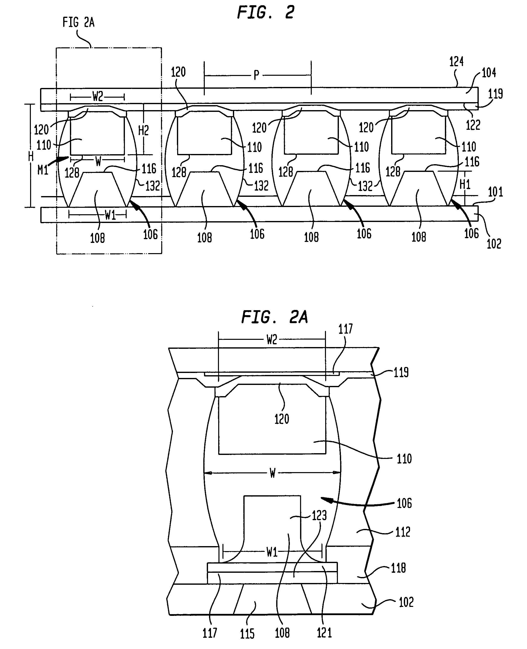
[0015]In an alternative of this embodiment, a fusible metal may be used to join the second posts to the first posts. Each of the first posts may have a diameter that is equal to a diameter of the second metal posts. Furthermore, a diameter of the first posts may be less than one-half of a pitch between each of the first posts.
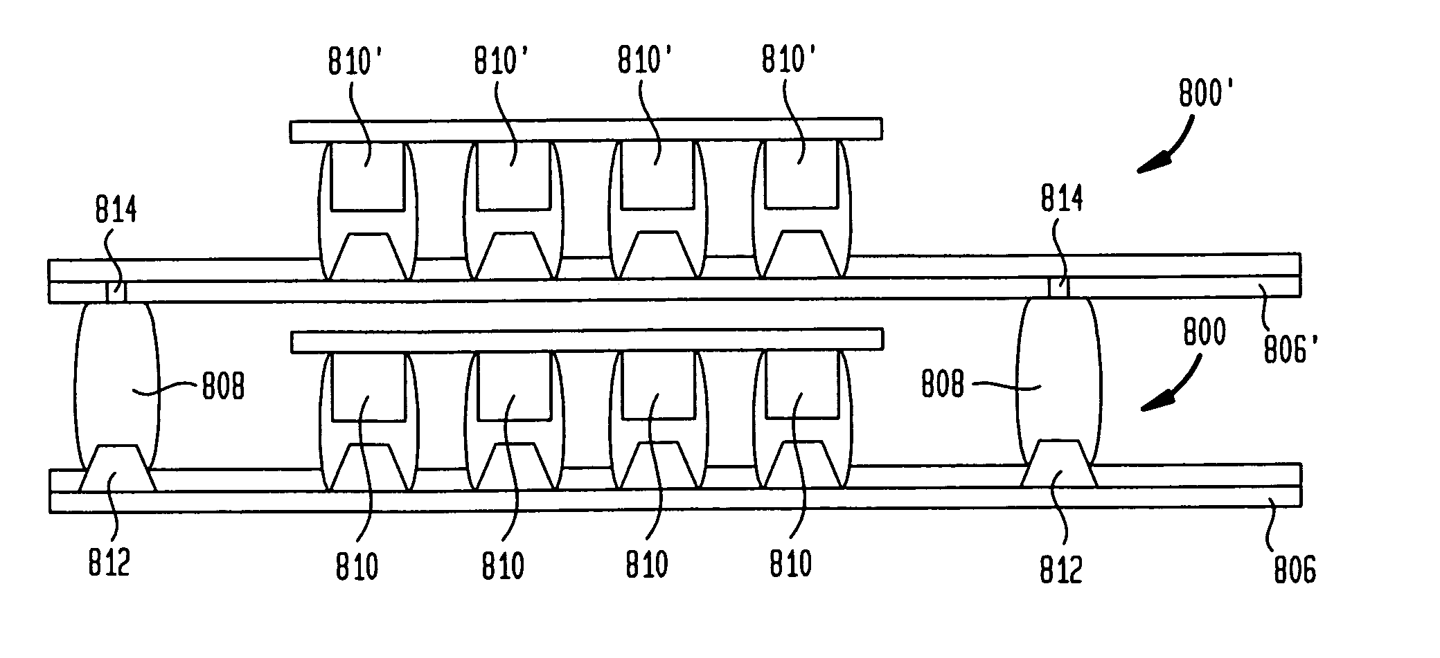
[0016]In another embodiment, a packaged microelectronic element includes a microelectronic element, a substrate, and a plurality of pillars extending between the microelectronic element and the substrate. Each of the plurality of pillars comprise a first metal post portion attached to the microelectronic element, a second metal post portion attached to the substrate, and a metal fusion portion, wherein the first and second metal portions are joined together. The plurality of pillars having a length not less than 50 microns. The height of the first and second metal post portions is at least half of the width.

Problems solved by technology

Additionally, underbump metallizations may underly the first bumps.

Method used


Image

  • Flip Chip Interconnection with double post
  • Flip Chip Interconnection with double post
  • Flip Chip Interconnection with double post

Examples


Embodiment Construction

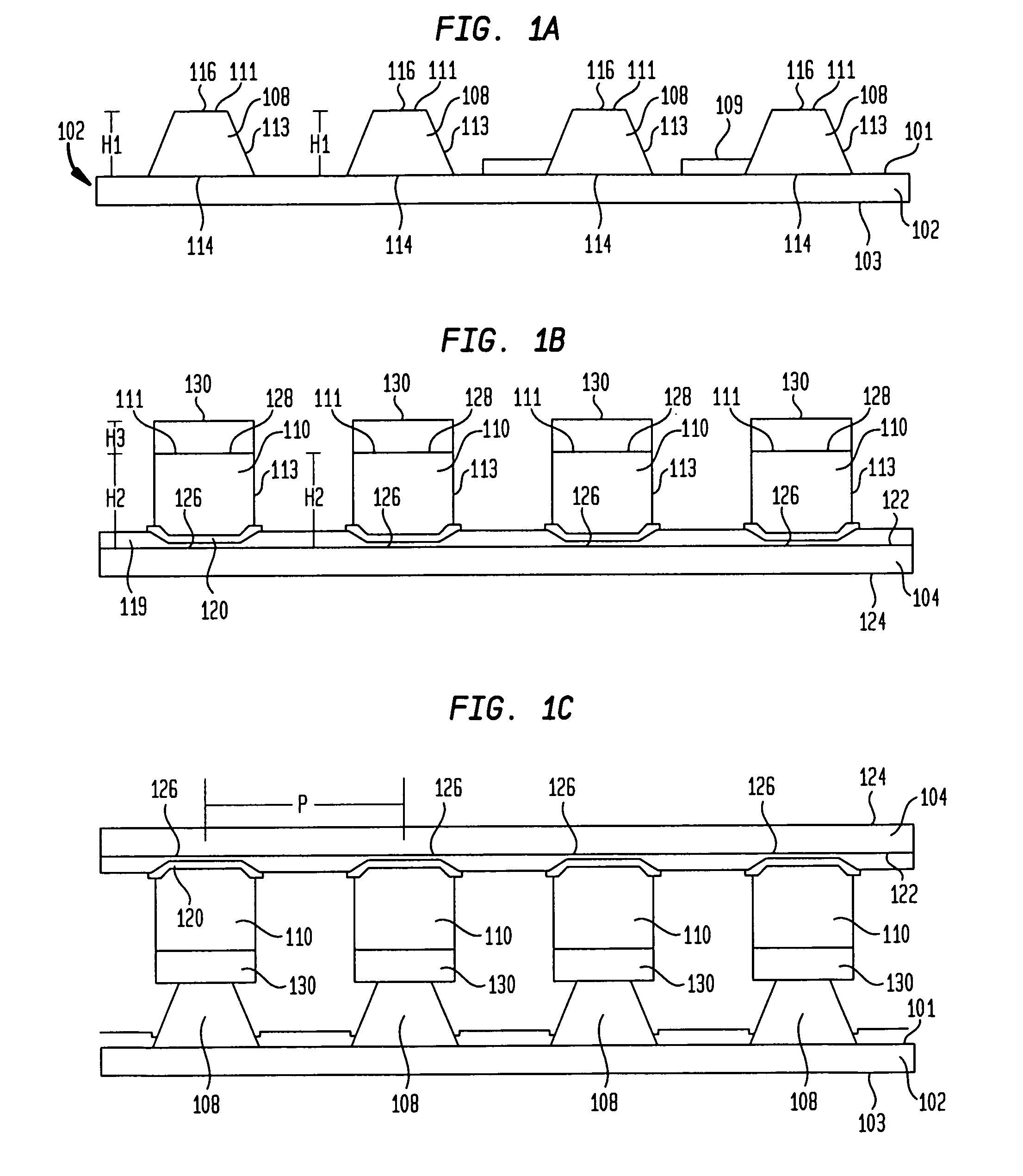
[0150]Reference is now made to FIGS. 1A-1C, which illustrate cross-sectional views of the components of the packaged microelectronic assembly 100 shown in FIG. 2. As shown, the packaged microelectronic assembly 100 includes a substrate 102, a microelectronic element 104 in a face down or flip chip position, and conductive columns 106 joining the substrate with the microelectronic element. The conductive columns include conductive bumps or posts 108 which protrude above a fact 105 of the substrate 102 that are aligned with conductive bumps or posts 110 protruding above a face 107 of the microelectronic element 104. The conductive columns 106 provide for increased height for chip-on-substrate packaging by increasing the standoff or vertical distance between the microelectronic element 104 and substrate 102, while at the same time allowing for a decrease in the center-to-center horizontal distance or pitch P between conductive columns 106. As will be discussed in further detail below, ...


PUM


Abstract

A packaged microelectronic assembly includes a microelectronic element having a front surface and a plurality of first solid metal posts extending away from the front surface. Each of the first posts has a width in a direction of the front surface and a height extending from the front surface, wherein the height is at least half of the width. There is also a substrate having a top surface and a plurality of second solid metal posts extending from the top surface and joined to the first solid metal posts.

Description

CROSS-REFERENCE TO RELATED APPLICATIONS[0001]This invention claims the benefit of the filing date of U.S. Provisional Patent Application No. 60 / 995,849 filed Sep. 28, 2007, the disclosure of which is hereby incorporated herein by reference.BACKGROUND OF THE INVENTION[0002]The present invention relates to microelectronic apparatuses and packaging microelectronic components for microelectronic packages and assemblies.[0003]Microelectronic devices generally comprise a thin slab of a semiconductor material, such as silicon or gallium arsenide, commonly called a die or a semiconductor chip. Semiconductor chips are commonly provided as individual, prepackaged units. In some unit designs, the semiconductor chip is mounted to a substrate or chip carrier, which is in turn mounted on a circuit panel, such as a printed circuit board.[0004]In one face of the semiconductor chip is fabricated the active circuitry. To facilitate electrical connection to the active circuitry, the chip is provided w...

Claims


Application Information

Patent Timeline
Patent Type & Authority Applications(United States)
IPC IPC(8): H01L23/488H01L21/50
CPCH01L21/563H01L23/49816H01L23/49822H01L23/49827H01L24/11H01L24/13H01L24/14H01L24/16H01L24/81H01L25/0657H01L25/105H01L2224/1147H01L2224/13016H01L2224/1308H01L2224/13082H01L2224/131H01L2224/13124H01L2224/13144H01L2224/13147H01L2224/13155H01L2224/16H01L2224/81001H01L2224/81136H01L2224/81193H01L2224/81203H01L2224/81894H01L2225/06517H01L2225/0652H01L2225/1023H01L2225/1058H01L2924/01013H01L2924/01022H01L2924/01029H01L2924/01032H01L2924/01033H01L2924/01078H01L2924/01079H01L2924/01082H01L2924/01322H01L2924/10253H01L2924/10329H01L2924/1532H01L2924/19041H01L2224/0558H01L2224/05624H01L2224/05644H01L2924/00013H01L2924/01005H01L2924/01006H01L2924/01019H01L2924/01024H01L2924/01047H01L2924/0105H01L2924/01074H01L2924/014H01L2224/81011H01L2224/831H01L21/4853H01L2224/13111H01L2224/16058H01L2224/16227H01L2224/16235H01L2224/73204H01L2224/81815H01L2224/8183H01L2224/16225H01L2224/13023H01L2224/13019H01L2224/13017H01L2224/13015H01L23/3178H01L2224/1412H01L2924/2064H01L2224/0401H01L2924/00014H01L2224/13099H01L2224/29099H01L2924/3841
Inventor KWON, JINSU
Owner TESSERA INC
Why Eureka
Try Eureka