Planar-like inductor coupling structure

Inactive Publication Date: 2009-06-11
IND TECH RES INST
View PDF8 Cites 41 Cited by
  • Summary
  • Abstract
  • Description
  • Claims
  • Application Information

AI Technical Summary

Benefits of technology

[0017]An exemplary example consistent with the present invention further provides a planar-like inductor coupling structure, which includes a first conductive layer, a second conductive layer, and a third conductive layer. The first conductive layer is in an insulating material layer and includes a first region and a second region, and the first and second regions have a partial overlapping region. The second conductive layer is in an insulating material layer and located on the first and second regions of the first conductive layer. The third conductive layer is in an insulating m

Problems solved by technology

However, if the filter device needs to be integrated in a chip design, due to the limitation of the chip area, the architecture of a quarter wavelength resonant cavity usually employed in a planar circuit cannot be adopted in the filter design, and only the capacitors and inductors embedded in the chip can be used to implement the architecture of the filter.
Therefore, it is the problem in a chip filter design in need of solution how to implement the coupling between filter resonant cavities.
However, the area of the inductors embedded in a chip is much larger than that of the capacitors, so the capacitor coupling needs additional capacitor devices and additional connecting lines as well.
However, since the number of metal layers in a semiconductor process is limited, the manners for producing a coupling mechanism between two embedded planar spiral inductors in a chip are limited. FIG. 2 shows a conventional spiral inductor coupling mechanism.
However, the strength of the coupling produced in FIG. 2 is weak. FIG. 3 shows another conventional spiral inductor coupling mechanism.
However, although the inductor coupling mechanism produced

Method used


Image

  • Planar-like inductor coupling structure
  • Planar-like inductor coupling structure
  • Planar-like inductor coupling structure

Examples


Embodiment Construction

[0033]Reference will now be made in detail to the present embodiments of the invention, examples of which are illustrated in the accompanying drawings. Wherever possible, the same reference numbers are used in the drawings and the description to refer to the same or like parts.

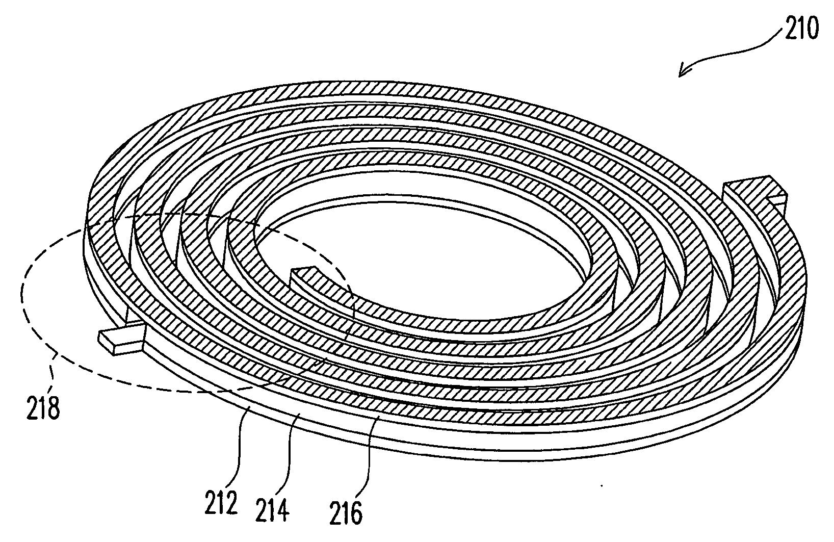
[0034]The circuit layout between two inductors adopted in the coupling mechanism of the present invention is basically different from the conventional design. In the present invention, an overlapping region between two planar inductors serves as the major inductor coupling mechanism, and the dimension of the inductor overlapping region may be easily adjusted. The larger overlapping area between the two inductors causes the larger inductor coupling effect. Thus, the coupling effect may be adjusted according to the design requirement, and meanwhile the additional chip design space may be saved due to the overlapping between the inductors. This inductor coupling mechanism can avoid the problems of a too small or ...


PUM


Abstract

A planar-like inductor coupling structure includes a first planar inductor embedded in an insulating material layer and a second planar inductor also embedded in the insulating material layer. The first planar inductor and the second planar inductor are substantially at the same height, and have a portion in a horizontal distribution serving as a coupled overlapping region with electric insulation from each other. In addition, the first planar inductor and the second planar inductor may be at different heights.

Description

CROSS-REFERENCE TO RELATED APPLICATION[0001]This application claims the priority benefit of Taiwan application serial no. 96147033, filed on Dec. 10, 2007. The entirety of the above-mentioned patent application is hereby incorporated by reference herein and made a part of this specification.BACKGROUND OF THE INVENTION[0002]1. Field of the Invention[0003]The present invention relates generally to a inductor coupling structure, especially relates to a planar-like inductor coupling structure.[0004]2. Description of Related Art[0005]With the developing trend of “light, thin, short, small,” and multi-function integration of electronic products, more and more circuit devices need to be integrated on a semiconductor chip, and a coupling mechanism between inductors becomes one of the indispensable devices in many semiconductor chip designs. No matter a signal conversion mechanism in various circuits, or a resonant cavity coupling in passive devices, the application of the coupling mechanism...

Claims


Application Information

Patent Timeline
IPC IPC(8): H01F5/00
CPCH01F17/0006H01F17/0013H01F2017/0046H01F38/14H01F19/08
Inventor LEE, MING-WEIWANG, CHIN-LI
Owner IND TECH RES INST
Why Eureka
Try Eureka