Optical sensor circuit and image sensor

an image sensor and optical sensor technology, applied in the field image sensors, can solve the problems of high impedance of the channel, inability to improve the s/n ratio by lengthening the exposure time, and the dynamic range cannot be largely widened, so as to achieve the effect of eliminating the output of optical sensor circuits (pixels), low illuminance and high sensitivity

Inactive Publication Date: 2009-06-11
HONDA MOTOR CO LTD
View PDF8 Cites 9 Cited by
  • Summary
  • Abstract
  • Description
  • Claims
  • Application Information

AI Technical Summary

Benefits of technology

[0034]According to the invention, in the initial state where a subthreshold current flows through the converting MOS transistor (Q1) and the transistor has transient characteristics, the high gate voltage value (VgH) of the converting MOS transistor (Q1) is switchingly set to the low gate voltage value (VgL), the potential difference ΔW (=W(Low)−W(High)) in each of plural optical sensor circuits is set by the difference between the high gate voltage value (VgH) of the converting MOS transistor (Q1) and the low gate voltage value (VgL). Therefore, a potential difference which does not depend on dispersion of the threshold voltages of the converting MOS transistors (Q1) constituting optical sensor circuits can be set. Accordingly, the potential differences ΔW among different optical sensor circuits in an image sensor can be made equal to one another. Since the potential difference ΔW can be arbitrarily set, a range showing a linear output region, and that showing a logarithmic output region can be arbitrarily controlled with respect to the terminal voltage (VC1) of the photoelectrical converting device which produces a sensor detection potential of the dark state of each optical sensor circuit (pixel). According to the configuration, dispersion of outputs among optical sensor circuits (pixels) can be eliminated.
[0035]From the above, according to the invention, in an optical sensor circuit which has linear and logarithmic output characteristics in accordance with the illuminance of incident light, a point of change between linear and logarithmic characteristic regions can be controlled, dispersion of potentials of the points of change among optical sensor circuits is stably eliminated, the S / N ratio at low illuminance or the like is high, the sensitivity is high, the dynamic range is wide, and the level of a residual image can be made low.

Problems solved by technology

Therefore, the circuit has a problem in that the dynamic range cannot be largely widened.
However, the photocurrent flows via the channel of the first MOS transistor Q21, and hence the S / N ratio cannot be improved by lengthening the exposure time unlike a storage type image sensor.
When the current flowing through the first MOS transistor Q21 is small, the impedance of the channel is high, and hence there arises a problem in that a residual image easily occurs.
However, the optical sensor circuit 301 has a problem in that, in the case where the circuit is configured as one pixel and such pixels are connected in a two-dimensional matrix pattern to form an imaging region and constitute a two-dimensional image sensor, a point of change between the region having a linear output characteristic and that having a logarithmic output characteristic is dispersed among pixels.

Method used


Image

  • Optical sensor circuit and image sensor
  • Optical sensor circuit and image sensor
  • Optical sensor circuit and image sensor

Examples


second embodiment

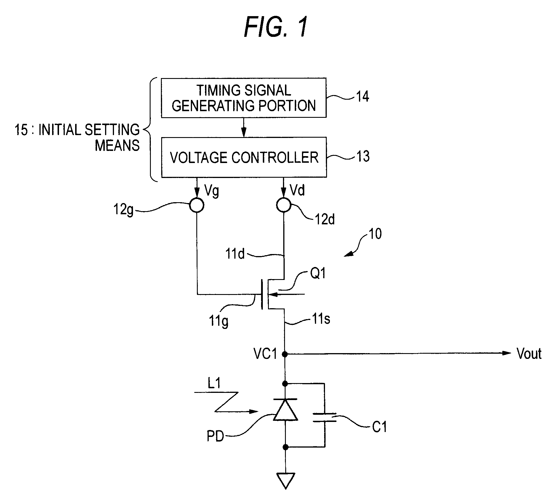
[0113]Next, the optical sensor circuit of the invention will be described with reference to FIG. 10. In FIG. 10, components which are substantially identical with those described with reference to FIG. 1 are denoted by the same reference numerals.

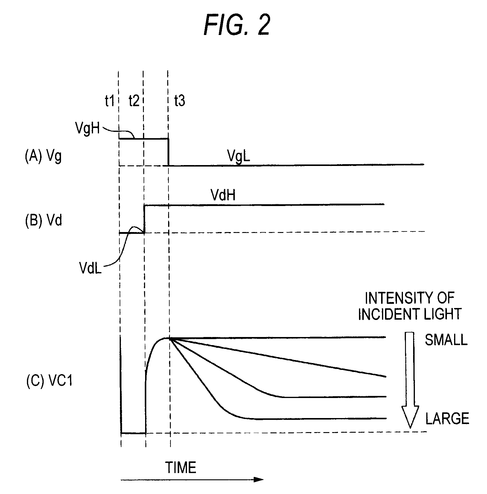
[0114]An optical sensor circuit 30 shown in FIG. 10 is configured so that the initial setting means 15 comprises switching means 31 which, when the gate voltage Vg of the MOS transistor Q1 is to be set to the high gate voltage value VgH on the basis of the initial setting means 15 configured by the voltage controller 13 and the timing signal generating portion 14, allows a voltage value relating to the high gate voltage value VgH to be arbitrarily set. According to the optical sensor circuit 30, when driving control signals Vg, Vd for driving various portions of the optical sensor circuit 10 are given as shown in FIG. 2, an electric signal corresponding to the light L1 is obtained.

[0115]As described above, when the gate voltage Vg of the MO...

fourth embodiment

[0126]The optical sensor circuit 60 further comprises, in the configuration of the optical sensor circuit 50 of the fourth embodiment, a capacitor C2 for accumulating charges, and the charge-moving fourth MOS transistor Q4. The fourth MOS transistor Q4 is a charge-moving MOS transistor for selectively moving charges between the capacitors C1 and C2. Based on the timing signals shown in FIG. 16, the above-described initial setting means 15 controls and sets the MOS transistors Q1 to Q4 in the following manner.

[0127]In a state where the charge-moving fourth MOS transistor Q4 is turned on by the voltage V5, the MOS transistors Q1 to Q3 are controlled and set.

[0128]The gate voltage V1 of the first MOS transistor Q1 is set to the high gate voltage value VgH, only for the predetermined time period between t1 to t3, the drain voltage V2 is set to the low drain voltage value VdL, only for the predetermined time period between t1 to t2, and the capacitor C1 of the photodiode PD and the capac...


PUM


Abstract

An optical sensor circuit has a photodiode PD, a MOS transistor Q1, a voltage controller 13 which supplies a gate voltage and a drain voltage to the transistor, etc. The voltage controller includes initial setting means 15. In the initial setting means, an electrostatic capacitance element of the photodiode is charged / discharged while setting a gate voltage of the transistor Q1 to a high gate voltage value VgH, only for a predetermined time period, and setting a drain voltage to a low drain voltage value VdL, only for a predetermined time period. Thereafter, the drain voltage is set to VdH, and, after elapse of a predetermined time period, the gate voltage is set to VgL. VgH, VdH, and VdL satisfy relational expressions of “VgH−VdH<Vth and VgH−VdL>Vth where Vth: a threshold voltage of the MOS transistor Q1”.

Description

TECHNICAL FIELD[0001]The present invention relates to an optical sensor circuit and an image sensor, and more particularly to an optical sensor circuit that is suitable for realizing a MOS image sensor which has linear and logarithmic output characteristics according to the illuminance of incident light, and in which the dynamic range is wide, and an image sensor which is produced by using the optical sensor circuit as one pixel.BACKGROUND ART[0002]Kinds of optical sensor circuits which form pixels of a MOS image sensor are classified into three circuits. The first optical sensor circuit is an optical sensor circuit having a linear output characteristic with respect to a change in the illuminance (intensity) of incident light, the second optical sensor circuit is an optical sensor circuit having a logarithmic output characteristic with respect to a change in the illuminance of incident light, and the third optical sensor circuit is an optical sensor circuit having a linear output ch...

Claims


Application Information

Patent Timeline
Patent Type & Authority Applications(United States)
IPC IPC(8): H04N5/335H04N5/355H04N5/357H04N5/374
CPCH01L27/14609H01L27/14643H04N3/155H04N5/3745H04N5/335H04N5/35518H04N5/35527H04N5/243H04N23/76H04N25/573H04N25/575H04N25/77H04N25/00
Inventor KAMIYAMA, TOMOYUKISHINOTSUKA, SUKEYUKIKUNIGAMI, MASAKIFURUKAWA, MAKOTO
Owner HONDA MOTOR CO LTD
Why Eureka
Try Eureka