[0010]The
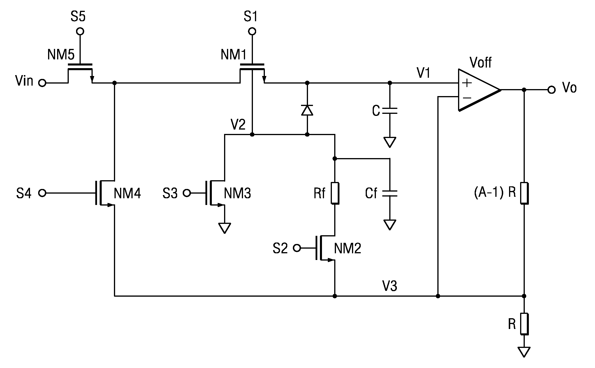
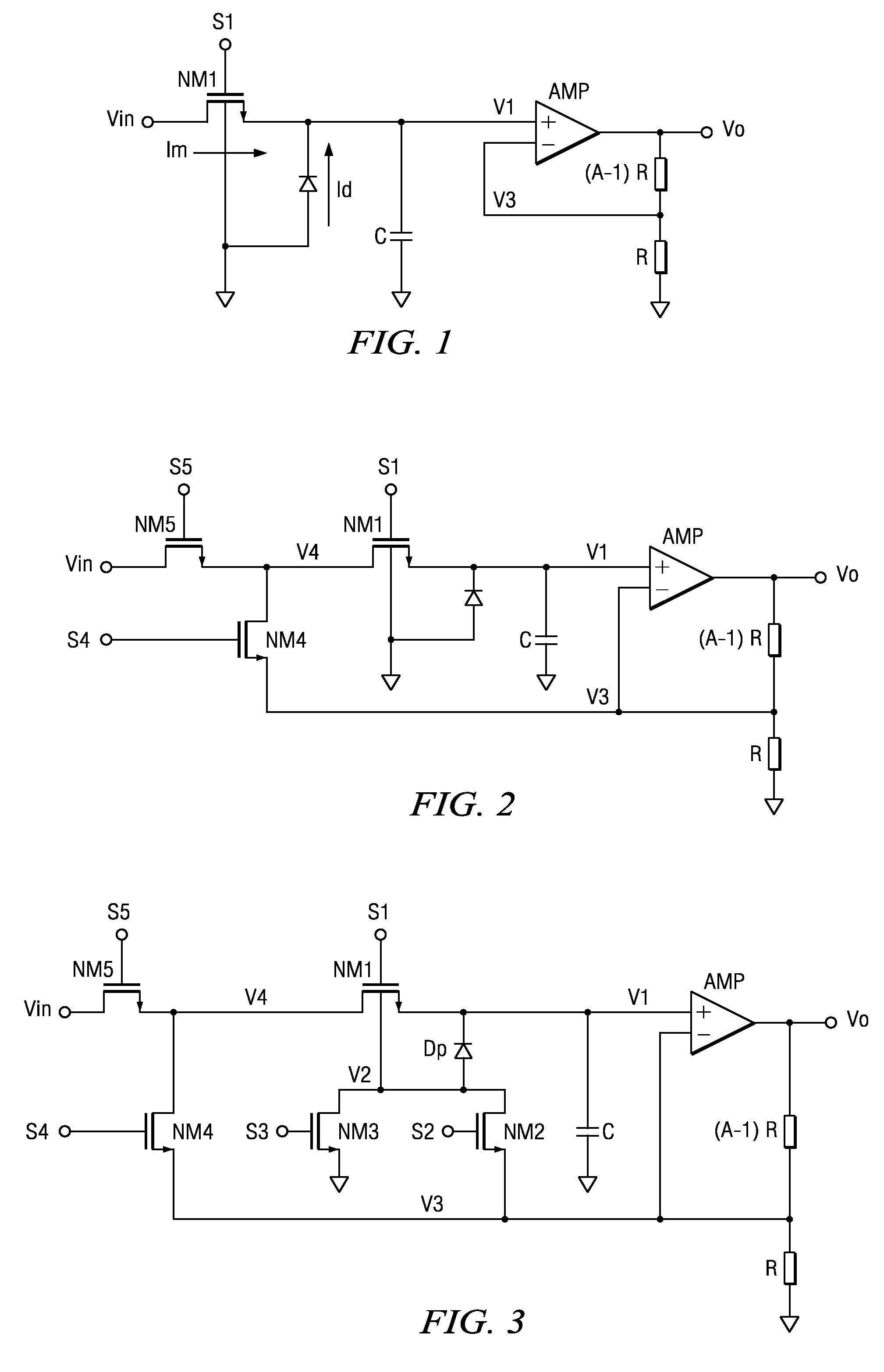
coupling of the bulk of the first transistor to the node having the required voltage level can be done by use of a second switch and a third switch coupled to the bulk of the first MOS transistor. The second and the third switches are controlled such that the bulk has a first voltage level during a hold phase and a to a second voltage level during a sample phase of the sample and hold stage. Preferably, the bulk of the first MOS transistor is controlled within the hold phase to have a voltage level that corresponds to the voltage level at the input of the voltage follower. If the voltage level of the bulk corresponds to the input of the voltage follower, the
voltage drop across the first MOS transistor is minimized and the leakage current becomes almost zero.
[0012]Advantageously, the integrated
electronic circuit further comprises a fourth switch and a fifth switch. The fifth switch is coupled between the input node and an input of the first switch, thereby providing an intermediate input node between the first switch and the fifth switch. Practically, the intermediate node is an additional node established between the first and the fifth switch by
coupling the fifth switch to the input node. The fourth switch is arranged such that the fourth switch connects a node with the intermediate input node in a
closed state, the node having a voltage level that corresponds to the voltage level at a negative input node of the
operational amplifier. The voltage of the negative input node of the
operational amplifier is substantially equal to the voltage of the positive input node of the
operational amplifier, if the operational
amplifier is configured as a voltage follower. Therefore, the node coupled to the negative input node can preferably be used to define the voltage level on the intermediate node. This arrangement provides that the
voltage drop across drain and source of the first MOS transistor is minimized during the hold phase. Using a fourth and a fifth switch in combination with the present invention allows almost all kinds of leakage currents to be avoided.
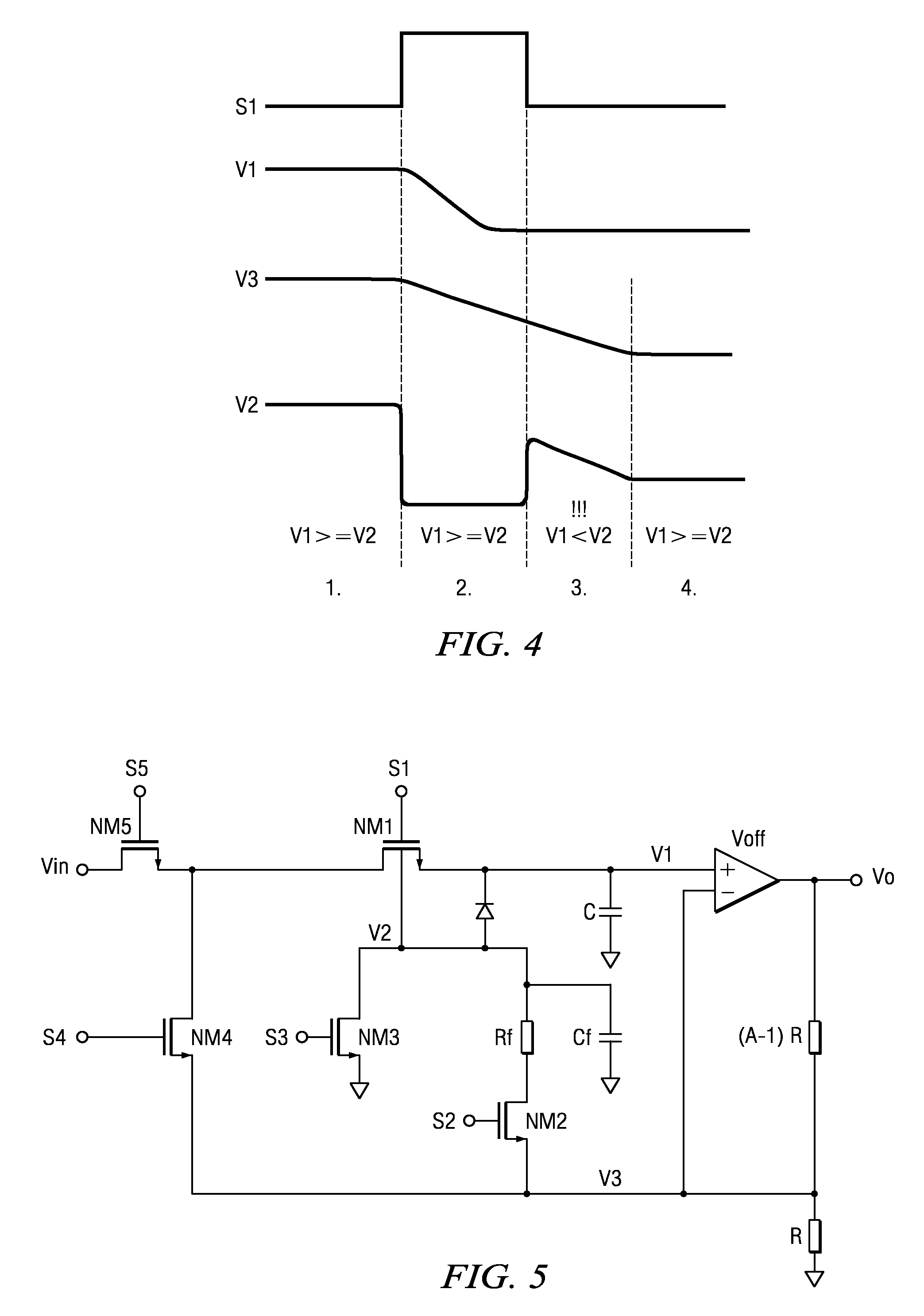
[0013]Further, a control stage can be provided in the integrated electronic device according to the present invention, which is adapted to control the switching of the second switch in a specific way. According to this aspect of the present invention, the second switch is coupled to the negative input of the operational
amplifier. In this situation, the second switch is controlled by the control stage such that it is only closed when the operational amplifier (or the voltage follower if another kind of voltage follower is used) has completely settled. Otherwise there would be a risk that glitches or changes in the voltage level at the negative input could interfere with the required voltage level of the bulk of the first MOS transistor. Therefore, it is necessary to close the second switch only after a time the operational amplifier needs to settle. Since the operational amplifier is connected as a voltage follower, the voltage level at the negative input node will be almost similar to the voltage level at the positive input node after the required
settling time. Therefore, the voltage level at the bulk becomes almost equal to the voltage level at the drain or the source (dependent on which of the source or the drain is connected to the positive input node of the operational amplifier) of the first MOS transistor. Further, there can be a
comparator with a built-in offset for detecting a minimum voltage difference between the positive input and the negative input of the operational amplifier. Such a
comparator can be adapted to monitor the correct and complete
settling of the operational amplifier. Only if the input voltages at the positive and negative input node of the operational amplifier are within a specific range, the second switch might be closed. A
low pass filter can be coupled to the bulk of the first MOS transistor for
smoothing the voltage level at the bulk. This is another possibility for minimizing glitches or unwanted variations of the voltage level of the bulk of the first transistor.
[0014]An aspect of the present invention also provides a method for sampling a voltage with a sample and hold stage. A first MOS transistor is closed in order to couple a sampling capacitor to an input voltage to be sampled. The first MOS transistor is then opened for holding the sampled voltage on the sampling capacitor. The voltage level at the bulk of the first MOS transistor is controlled while the first MOS transistor is open, such that the voltage level of the bulk is equal or close to the sampled voltage level on the sampling capacitor. Accordingly, the
voltage drop across the first MOS transistor, in particular between bulk and the side which is coupled to the sampling capacitor is minimized and leakage current is avoided. The step of controlling the voltage level at the bulk, in particular
coupling the bulk to a node with a required voltage level corresponding to the input voltage level at the voltage follower's input can be delayed for a specific
settling time the voltage follower (or the operational amplifier) needs to settle.

