Integrated circuit device core power down independent of peripheral device operation

a technology of integrated circuits and peripheral devices, applied in the field of digital computer systems, can solve the problems of high overhead, inability to retain the current processor state information necessary to continue execution, and only performing useful work of integrated circuits providing the functionality of devices, so as to reduce the requirements for signal trace routing

Active Publication Date: 2009-06-18
NVIDIA CORP
View PDF99 Cites 29 Cited by
  • Summary
  • Abstract
  • Description
  • Claims
  • Application Information

AI Technical Summary

Benefits of technology

[0009]Embodiments of the present invention provides a method and system for powering down an integrated circuit device for reduced standby power consumption while retaining the integrity of the operating state. Embodiments of the present invention further provide a solution for powering down the integrated circuit device without imposing burdensome trace watering requirements on the integrated circuit die layout.
[0011]In this manner, the signal state of the input output pins can be maintained as one or more functional blocks of the integrated circuit device are powered down. Upon exit from sleep mode (e.g., wake up), the input output pins can resume being driven by the one or more functional blocks. Additionally, this capability is provided without requiring the routing of multiple signals from a special power domain to the input output pin, which greatly reduces signal trace routing requirements. For example, embodiments of the present invention enabled a wake-up when one of a designated set of inputs transitions state. This allows the integrated circuit device to use the same pins that are used to recognize events during normal operation as wake pins to transition the device out of deep sleep.

Problems solved by technology

Generally, is estimated that that the integrated circuits providing the functionality of the device is only performing useful work approximately 2% of the time while the device is in standby mode.
A primary reason for not applying this technique to CPUs, has been the difficulty in being able to retain the current processor state information necessary to continue execution after coming out of the standby mode.
In such a case there is the overhead required in transferring the state to and from the external storage mechanism.
Even if the battery powered device had a hard disk drive, and many don't, the time consuming state transfer would not meet the real time response requirements of the application when the device needs to wake up to respond to a new event.
Other issues are presented when the functionality of a device is implemented by a system-on-a-chip (SOC) integrated circuit.
This causes a problem since some peripherals need particular values to be set at their inputs (which are connected to the outputs of the SOC) to hold a safely inactive state.
This problem is further exacerbated by the heavy use of pin-muxing or sharing, in which a single pin can have multiple functions in different designs by different customers.
While pin-muxing provides a way to put more features in each chip and allows the chip to be more suitable for a wide range of designs, it precludes knowing exactly at IC design time what each pin will be used for.
This is a workable solution, but has a problem that since normally the signals that control these functions come from the core of the CPU, they will not be present when the core is powered down in deep sleep mode.
However the big problem is that it requires multiple signals from the portion of the chip that is in the special power domain to each pad, this can cause traces to be required.
These pad control signals must also be powered by the AO rail, which complicates the distribution of this AO rail or the routing of these pad control signals.
The benefits of a low power strategy cannot be fully realized if this mechanism is not transparent to the external environment.

Method used


Image

  • Integrated circuit device core power down independent of peripheral device operation
  • Integrated circuit device core power down independent of peripheral device operation
  • Integrated circuit device core power down independent of peripheral device operation

Examples


Embodiment Construction

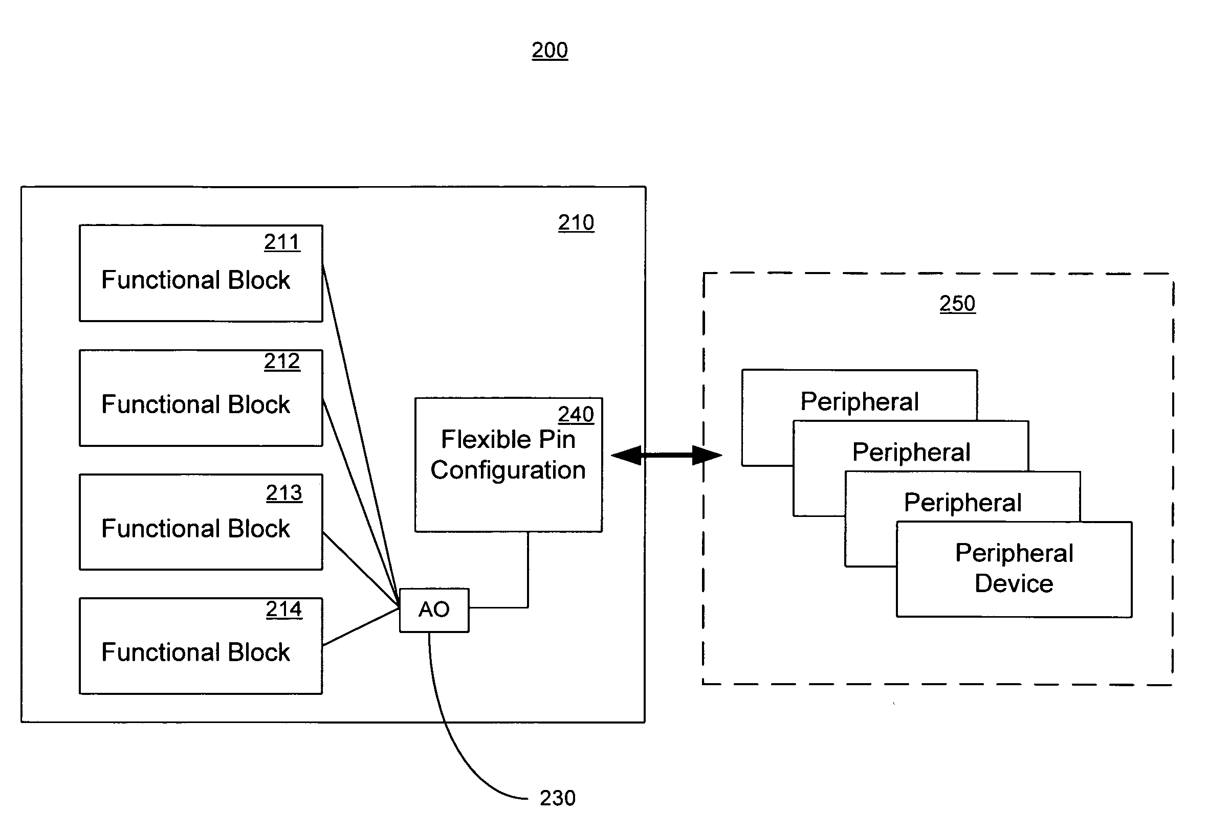
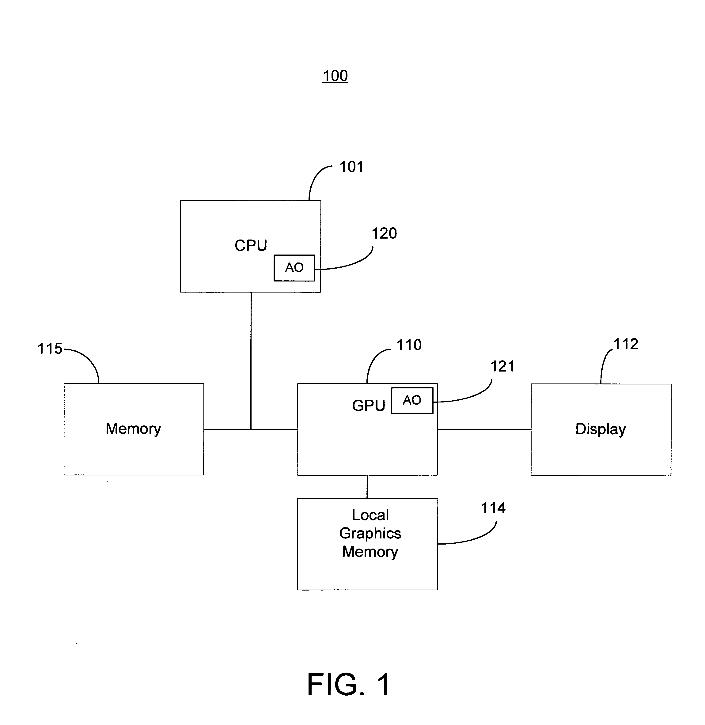
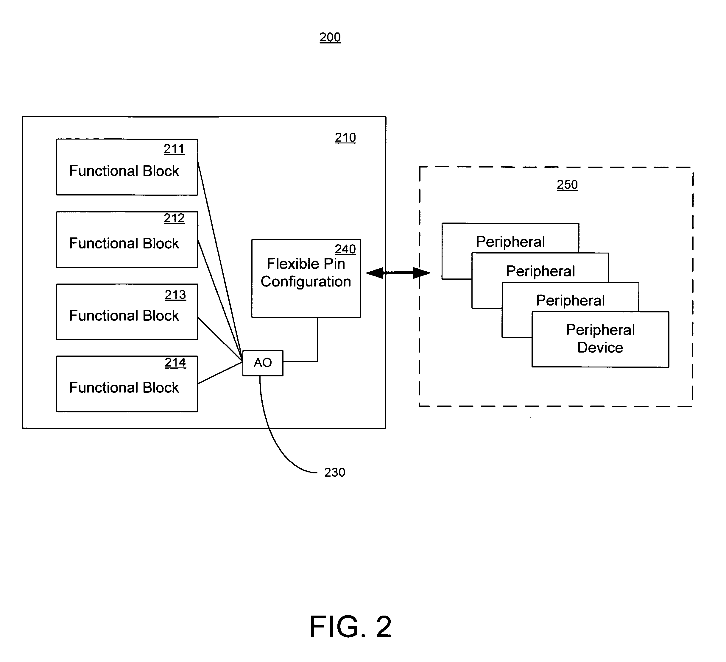
[0019]Reference will now be made in detail to the preferred embodiments of the present invention, examples of which are illustrated in the accompanying drawings. While the invention will be described in conjunction with the preferred embodiments, it will be understood that they are not intended to limit the invention to these embodiments. On the contrary, the invention is intended to cover alternatives, modifications and equivalents, which may be included within the spirit and scope of the invention as defined by the appended claims. Furthermore, in the following detailed description of embodiments of the present invention, numerous specific details are set forth in order to provide a thorough understanding of the present invention. However, it will be recognized by one of ordinary skill in the art that the present invention may be practiced without these specific details. In other instances, well-known methods, procedures, components, and circuits have not been described in detail ...


PUM


Abstract

In an integrated circuit device, a circuit for maintaining asserted values on an input output pin of the device when a functional block of the device is placed in a sleep mode. The circuit includes an interface for coupling a functional block of a processor to an input and output pin and an output storage element coupled to the interface for storing a current value of the input output pin. The circuit further includes a sleep mode enable for controlling the output storage element to store the current value of the input output pin prior to the functional block being entering a sleep mode and cause the current value of the input output pin to remain asserted after the functional block is in sleep mode. The sleep mode enable is also to deactivate the storage element when the sleep mode is exited.

Description

FIELD OF THE INVENTION[0001]The present invention is generally related to digital computer systems.BACKGROUND OF THE INVENTION[0002]One of the important features of integrated circuits deigned for portable applications is their ability to efficiently utilize the limited capacity of the battery power source. Typical applications include cellular telephones and personal digital assistants (PDAs), which might have a Lithium ion battery or two AAA alkaline batteries as the power source. Users have come to expect as much as three to four weeks of standby operation using these devices. Standby operation refers to the situation where the cellular phone, handheld device, etc. is powered on but not being actively used (e.g., actively involved in a call). Generally, is estimated that that the integrated circuits providing the functionality of the device is only performing useful work approximately 2% of the time while the device is in standby mode.[0003]Removing the power supply from selected...

Claims


Application Information

Patent Timeline
Patent Type & Authority Applications(United States)
IPC IPC(8): H03K3/02
CPCG06F1/3203G06F1/3287Y02B60/1278G06F1/22Y02B60/1282Y02B60/32Y02D10/00Y02D30/50G06F13/4068
Inventor HENDIN, NEILNAJAM, ZAHIDLE PROVOST, STEPHANESMITH, BRIAN
Owner NVIDIA CORP
Why Eureka
Try Eureka