Method of forming a CMOS structure having gate insulation films of different thicknesses

a technology of gate insulation and cmos, which is applied in the direction of semiconductor devices, digital storage, instruments, etc., can solve the problems of increasing the power dissipation of mos transistors during standby periods, increasing the leakage current (tunnel leakage current), etc., to reduce the power dissipation significantly, less leakage current magnitude, and eliminate adverse influence or affection

Inactive Publication Date: 2008-09-23
TESSERA ADVANCED TECH
View PDF28 Cites 28 Cited by
  • Summary
  • Abstract
  • Description
  • Claims
  • Application Information

AI Technical Summary

Benefits of technology

[0011]Another approach is known which suppresses a sub-threshold source-to-drain leakage current by potentially raising the threshold value of MOS transistors. However, even with use of such approach, it stays impossible in principle to reduce standby power dissipation due to the flow of source-to-gate tunnel current.
[0030]In accordance with a further aspect of the invention, a semiconductor integrated circuit device responsive to receipt of an input signal having a specified amplitude voltage Vcc2 is arranged to include a level converter circuit for generating and issuing an in-chip signal by potentially reducing the amplitude voltage of an input signal, wherein leakage current occurrable between the gate and source or between the gate and drain of a MOS transistor accepting the in-chip signal is greater than that in another MOS transistor receiving the input signal.

Problems solved by technology

However, this does not come without accompanying a “trade-off” penalty: When the MOS gate insulation film becomes too thinner, a tunnel current begins flowing therethrough.
This can result in an increase in leakage current (tunnel leakage current), such as a source-to-gate current or drain-to-gate current, which inherently does never take place in standard MOS transistors.
Such increase in tunnel leakage current in turn leads to an increase in power dissipation of MOS transistors during standby periods thereof.

Method used


Image

  • Method of forming a CMOS structure having gate insulation films of different thicknesses
  • Method of forming a CMOS structure having gate insulation films of different thicknesses
  • Method of forming a CMOS structure having gate insulation films of different thicknesses

Examples


first embodiment

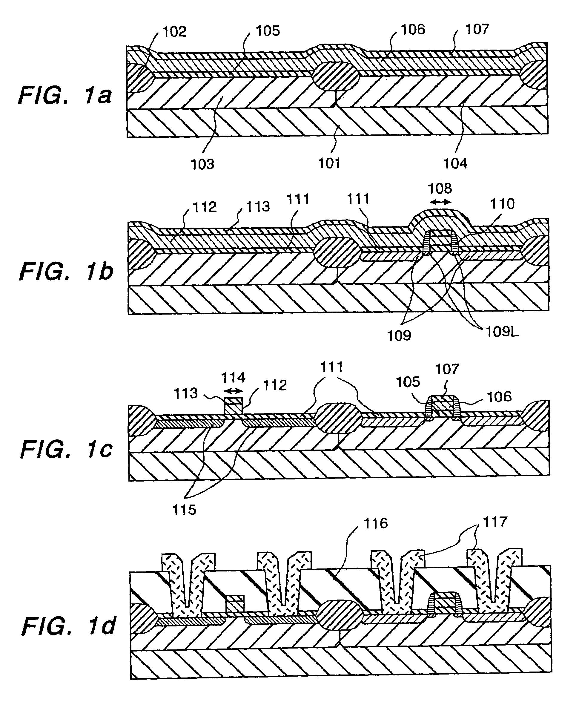
[0088]The first embodiment will now be explained in conjunction with FIG. 1. This embodiment is drawn to the manufacture of an exemplary IC device attaining copresence of a tunnel current available MOS transistor and a tunnel current depleted MOS transistor without any substantive flow of tunnel current therein on the same chip substrate by differing the thickness of gate insulation film between them. While this embodiment is intended to fabricate such two different kinds of gate insulation films by use of both p-type MOS transistors and n-type MOS transistors, cross-sections presented in FIG. 1 assume use of p-type MOS transistors only for purposes of reducing complexity of illustration. An n-type silicon substrate 101 is prepared having a top surface on which an element isolation dielectric region 102 made of a thermal oxide film of 300 nm thick is formed. In the substrate surface, n-type impurity-doped layers 103 and 104 are formed. These impurity layers 103, 104 are 1×10¹⁷ atoms...

second embodiment

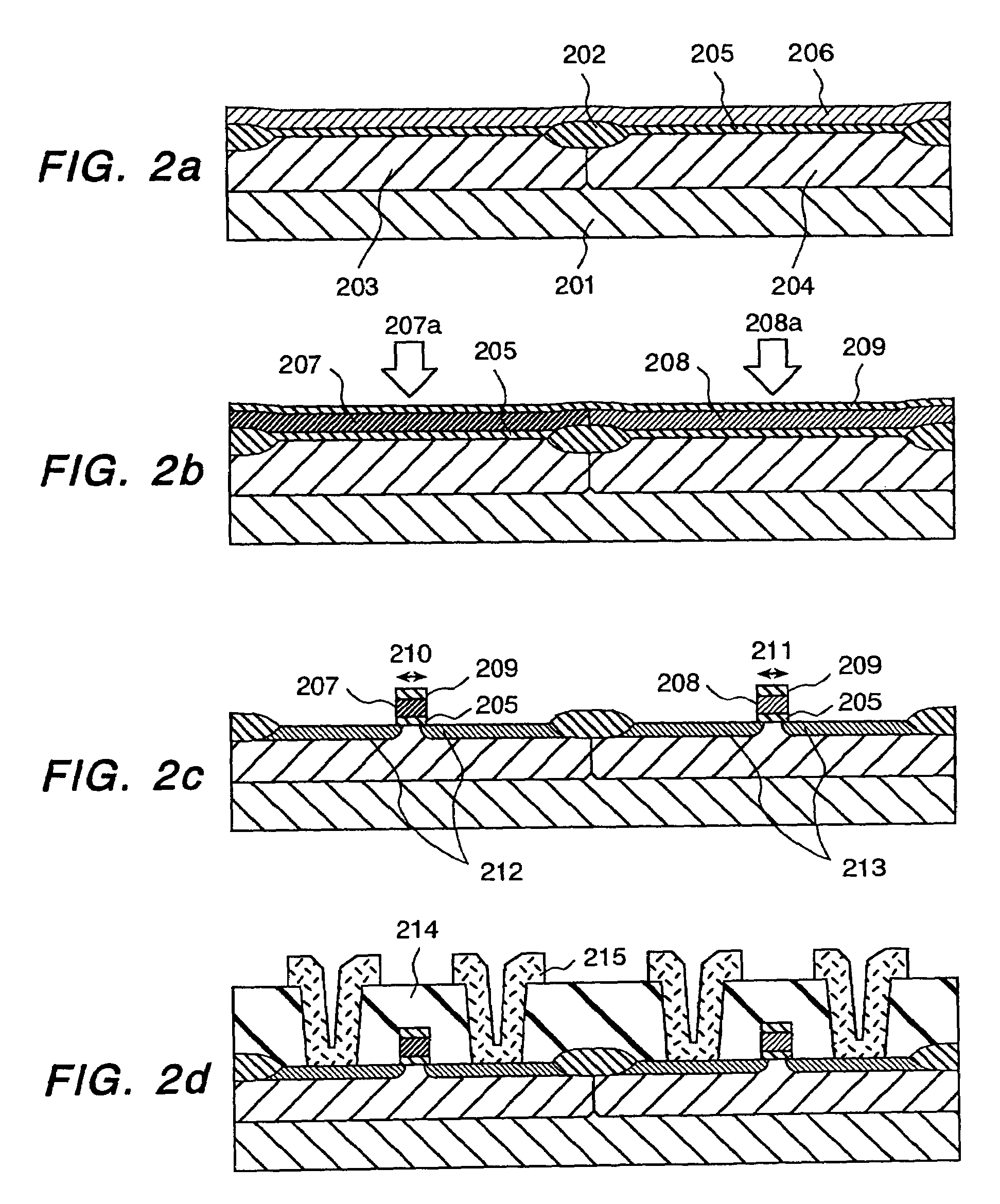
[0106]A second embodiment is shown in FIG. 2, which is directed to one exemplary manufacturing method of an IC chip having on the same substrate different kinds of MOS transistors: tunnel-current available MOS transistors permitting flow of a tunnel current therein resulting from a change of impurity concentration at gate and source portions, and tunnel-current absent MOS transistors permitting no substantive tunnel current flow therein. In this embodiment the cross-sections of p-type MOS transistors alone are illustrated in FIG. 2 in the same manner as that in the previous embodiment (FIG. 1). An n-type silicon substrate 201 is prepared on which an element isolation dielectric region 202, an n-type impurity layer 203 and an n-type impurity layer 204 are formed as shown. Here the n-type layer 203 is devoted to provision of a well region of transistors for use in constituting a main circuit whereas n-type layer 204 is for a well of power-supply intercept MOS transistors which selecti...

third embodiment

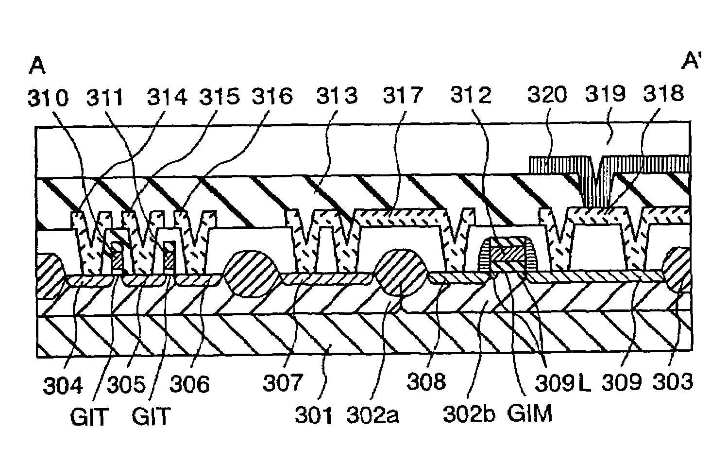
[0111]A third embodiment will now be described with reference to FIGS. 3 and 4. FIGS. 3 and 4 are diagrams each showing one practical configuration of a semiconductor integrated circuit device embodying the invention, wherein FIG. 3 is a layout depiction of this embodiment whereas FIG. 4 is a cross-sectional view of the layout taken along line A-A′ of FIG. 3. The IC device is an example having a series combination of two NAND gate circuits.

[0112]In FIG. 3, MOS transistors MP and MN are those for power supply intercept (for use with a control circuit), and measure 10 nm in gate insulation film thickness although these remain operable with 5-nm gate insulation film thickness. MOS transistors TP and PN are for use with a logic circuit (main circuit), and are 3.5 nm in gate insulation film thickness. In this way, this embodiment employs two kinds of MOS transistors with different gate insulation film thickness values. Here, the gate length LM of gate insulation film thickness-increased ...


PUM


Abstract

The semiconductor integrated circuit device employs on the same silicon substrate a plurality of kinds of MOS transistors with different magnitudes of tunnel current flowing either between the source and gate or between the drain and gate thereof. These MOS transistors include tunnel-current increased MOS transistors at least one of which is for use in constituting a main circuit of the device. The plurality of kinds of MOS transistors also include tunnel-current reduced or depleted MOS transistors at least one of which is for use with a control circuit. This control circuit is inserted between the main circuit and at least one of the two power supply units.

Description

[0001]This is a continuation application of U.S. Ser. No. 10 / 263,705, filed Oct. 4, 2002,now abandoned which is a continuation application of U.S. Ser. No. 09 / 852,793, filed May 11, 2001 (now U.S. Pat. No. 6,500,715); which is a divisional application of U.S. Ser. No. 09 / 155,801, filed Oct. 6, 1998 (now U.S. Pat. No. 6,307,236 B1); which is a 371 of PCT / JP97 / 01191, filed Apr. 8, 1997.TECHNICAL FIELD[0002]The present invention relates generally to semiconductor integrated circuit (IC) devices configured using metal oxide semiconductor (MOS) transistors, and more particularly to a semiconductor IC device which employs specific MOS transistors with a gate insulation film thin enough to permit flow of tunnel current therein and which is adaptable for use with low-power circuitry operable with low voltages of 2 volts or less.BACKGROUND ART[0003]One prior known semiconductor integrated circuit device employing highly miniaturized MOS transistors fabricated by microelectronics fabrication ...

Claims


Application Information

Patent Timeline
Patent Type & Authority Patents(United States)
IPC IPC(8): H01L29/72H01L21/8234H01L27/088
CPCH01L21/82345H01L21/823468H01L27/088H01L29/42364H01L27/0883H01L21/823462Y10S977/936Y10S438/981B82Y99/00H01L21/823857H01L21/82385
Inventor MATSUZAKI, NOZOMUMIZUNO, HIROYUKIHORIGUCHI, MASASHI
Owner TESSERA ADVANCED TECH
Why Eureka
Try Eureka