

Transmission electron microscopy analysis method using focused ion beam and transmission electron microscopy sample structure
a technology of transmission electron microscopy and analysis method, which is applied in the direction of material analysis using wave/particle radiation, semiconductor/solid-state device testing/measurement, instruments, etc., can solve the problem of inability to make analysis on a specific point precisely, and achieve the effect of improving analysis accuracy and reliability and reducing analysis failure ra
- Summary
- Abstract
- Description
- Claims
- Application Information
AI Technical Summary
Benefits of technology
Problems solved by technology
Method used
Image

Examples
Embodiment Construction
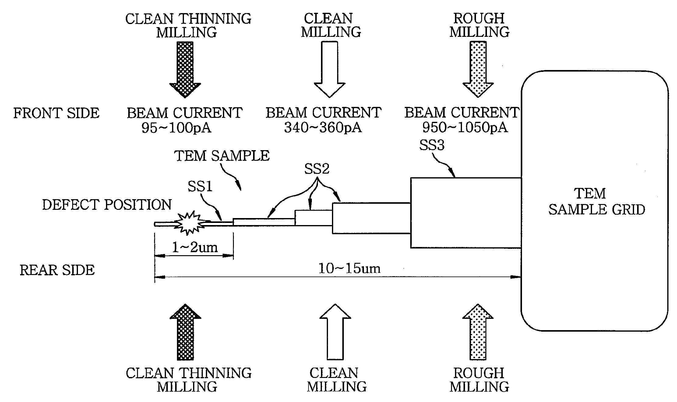
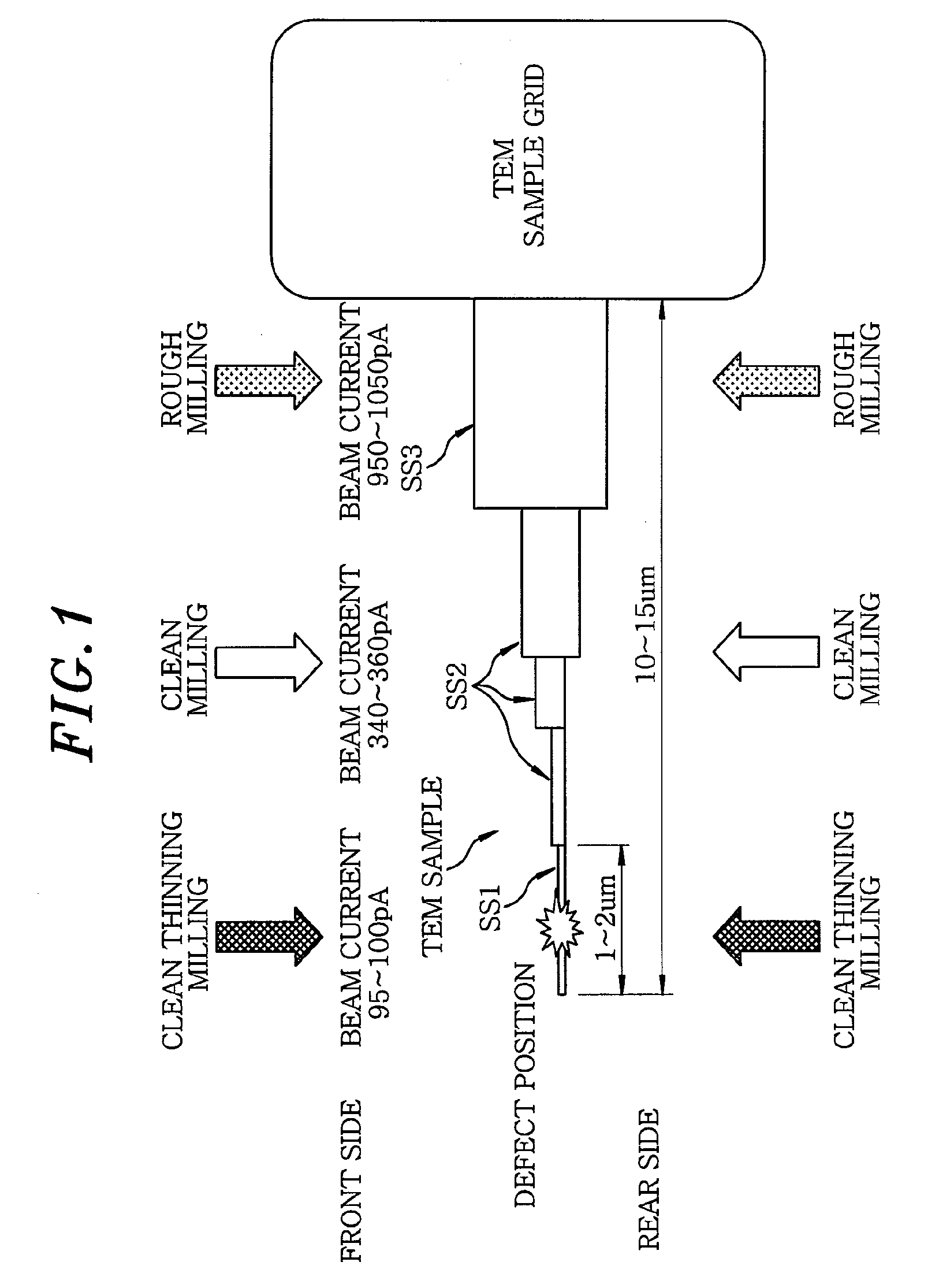
[0008]In general, example embodiments of the invention relate to an a TEM analysis method using FIB and a TEM sample structure, in which the TEM sample is divided into a plurality of analysis regions having different thicknesses therebetween to reduce an analysis failure rate and improve analysis accuracy and reliability.
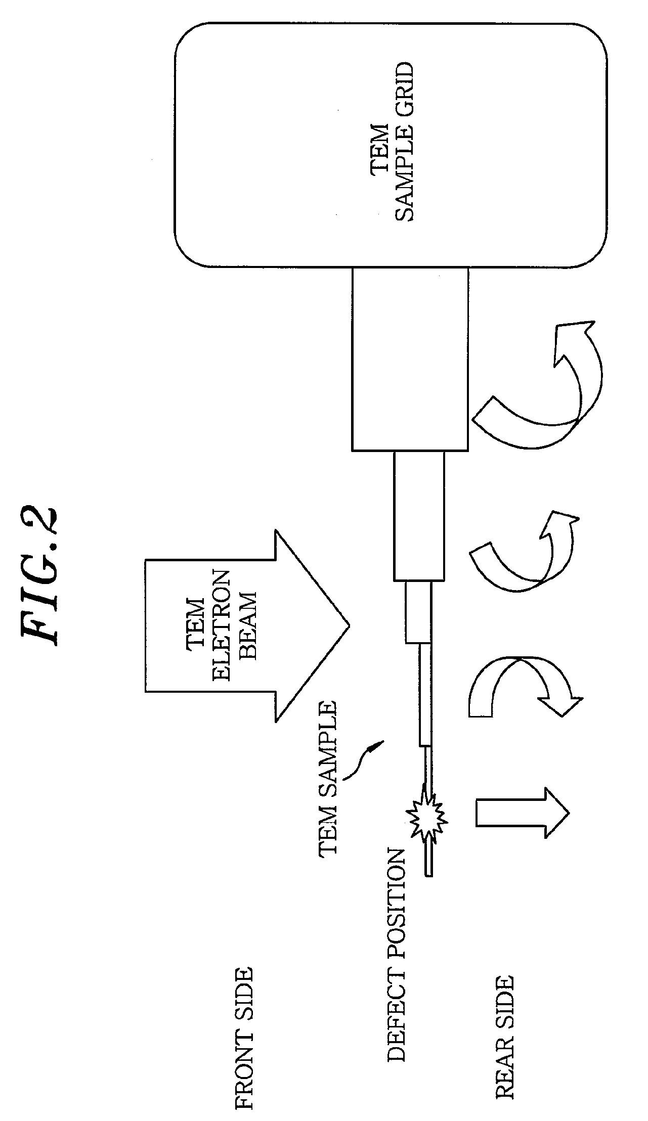
[0009]In accordance with a first embodiment, there is provided a TEM analysis method using FIB, the method including: dividing a TEM sample into a plurality of analysis regions; determining an FIB beam current for each of the analysis regions; performing FIB milling on each of the analysis regions by using the determined FIB beam current; and loading the TEM sample onto a TEM sample grid and transmitting a TEM electron beam on the TEM sample to perform the TEM analysis.
[0010]The analysis regions may be divided into a first analysis region through which the TEM electron beam passes roughly, a second analysis region through which the TEM electron beam passes more clea...
PUM
| Property | Measurement | Unit |
|---|---|---|
| current | aaaaa | aaaaa |
| current | aaaaa | aaaaa |
| current | aaaaa | aaaaa |
Abstract
Description
Claims
Application Information