Reading configuration data from internal storage node of configuration storage circuit

a configuration storage circuit and configuration data technology, applied in the field of configuration integrated circuits, can solve the problems of increasing the complexity of the configuration, reducing the performance gain of configuration setup time or resources, and introducing additional circuit complexity, so as to reduce the number of storage elements.

Active Publication Date: 2009-07-02
ALTERA CORP
View PDF22 Cites 22 Cited by
  • Summary
  • Abstract
  • Description
  • Claims
  • Application Information

AI Technical Summary

Benefits of technology

[0013]A context switcher that can switchably connect to different sets of configuration storage circuits can provide different sets of configuration data sets to the configurable circuit, in order to allow the configurable circuit to reconfigure while the IC is operating. In some embodiments, the context switcher can “loop” through several (e.g., four, six, eight, etc.) configuration data sets (i.e., by changing its connections to the configuration storage circuits based on a particular looping pattern) at a particular rate, so that the configurable circuit can potentially reconfigure its operation at that rate.
[0015]The clocked storage circuit of some embodiments includes a storage cell that stores configuration data. In some embodiments, the clocked storage circuit receives a clock signal that in a first state enables the storage cell to receive configuration data that the storage circuit receives, and in a second state causes the storage cell to maintain and store the configuration data that the storage cell received while the clock was in the first state. The storage cell can maintain the stored configuration data for a period of time even when the input to the storage circuit changes. In some embodiments, the clock signal enables at least one transistor that connects the storage cell to a power state (e.g., ground). Instead of using a clock signal, some embodiments employ a pulse signal, which may be derived from a clock signal.
[0019]In some embodiments, the direct connection is received by a single input line of an interconnect circuit of the context switcher. This input line may be implemented as a single physical bit line or a differential pair of bit lines. The interconnect circuit has one or more other inputs that also directly connect to the internal storage nodes of one or more other storage circuits. The interconnect circuit then can controllably switch between different inputs to provide the configuration data values appearing on these inputs along the interconnect circuit's output, which again can be implemented as a single physical bit line or a pair of differential bit lines. In some embodiments, the interconnect circuit switches between different inputs at a particular rate, so that the context switcher can provide different configuration data sets to the configurable circuit at the particular periodic rate.

Problems solved by technology

Such use of the dual ported RAM introduces additional circuit complexity, such as multiplexers and configuration values to control the multiplexer in alternatively switching between the odd and even cycles.
Attempts to reduce the size of such configuration data supplying circuitry include tradeoffs that ultimately have yielded minimal performance gain in either configuration setup time or resources used.

Method used


Image

  • Reading configuration data from internal storage node of configuration storage circuit
  • Reading configuration data from internal storage node of configuration storage circuit
  • Reading configuration data from internal storage node of configuration storage circuit

Examples


Embodiment Construction

[0093]In the following description, numerous details are set forth for purpose of explanation. However, one of ordinary skill in the art will realize that the invention may be practiced without the use of these specific details. For instance, not all embodiments of the invention need to be practiced with the specific number of bits and / or specific devices (e.g., master latches) referred to below. In other instances, well-known structures and devices are shown in block diagram form in order not to obscure the description of the invention with unnecessary detail.

I. Overview

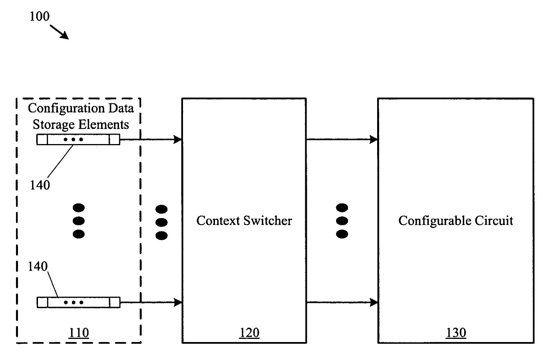
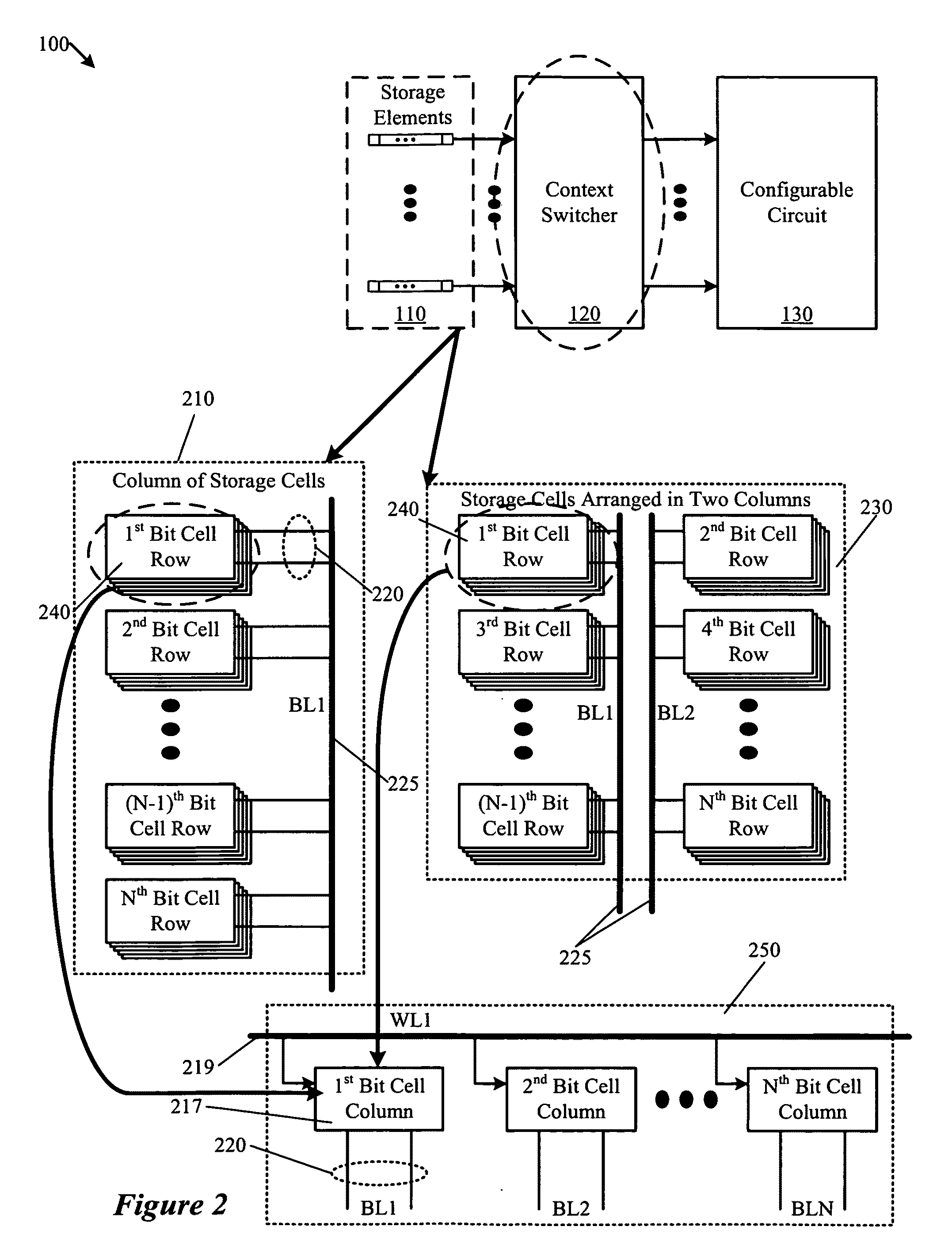
[0094]Different embodiments of the invention provide different context switchers for retrieving configuration data from configuration data storage elements (e.g., SRAM cells) and supplying the retrieved data to a configurable circuit (e.g., configurable interconnect circuit or configurable logic circuit) of an IC. In some embodiments, the context switching circuitry re-times the data coming from the configuration st...


PUM


Abstract

Some embodiments provide an IC with configuration context switchers. The IC includes several configurable circuits, each of which configurably performs one of several operations at any given time, based on the configuration data set that it receives at that time. The IC includes several storage circuits for storing several configuration data sets for each of the configurable circuits. The IC also includes a context switching interconnect circuit for switchably connecting the configurable circuit to different sets of storage circuits to receive different sets of configuration data sets. The context switcher includes one or more stages for re-timing the data coming from the configuration storage elements. The stages can include interconnect circuitry or storage circuitry. Some embodiments build one of the stages in the configuration data storage elements. Some embodiments encode the configuration data bits and hence utilize a decoder in the context switcher to decode the encoded configuration data.

Description

CLAIM OF BENEFIT TO PRIOR APPLICATIONS[0001]This application claims benefit to U.S. Provisional Patent Application 60 / 970,504, entitled “Space Time Context Register,” filed Sep. 6, 2007. This United States Provisional patent application is incorporated herein by reference.FIELD OF THE INVENTION[0002]The invention relates to configurable integrated circuits (ICs). More particularly, this invention relates to a configuration cycle data decoder and synchronization circuit.BACKGROUND[0003]An IC is a device that includes numerous electronic components (e.g., transistors, resistors, diodes, etc.) that are embedded typically on the same substrate, such as a single piece of semiconductor wafer. These components are connected with one or more layers of wiring to form multiple circuits, such as Boolean gates, memory cells, arithmetic units, controllers, decoders, etc. An IC is often packaged as a single IC chip in one IC package, although some IC chip packages can include multiple pieces of s...

Claims


Application Information

Patent Timeline
Patent Type & Authority Applications(United States)
IPC IPC(8): H03K19/173
CPCG06F15/7867G11C7/1045H03K19/17748H03K19/17752H03K19/17768H03K19/17732H01L2224/32145H01L2224/32225H01L2224/48227H01L2224/73265H01L2924/15311H01L2224/48091H03K19/0008H01L2924/00H01L2924/00014H03K3/0372
Inventor VOOGEL, MARTINREDGRAVE, JASONCHANDLER, TREVIS
Owner ALTERA CORP
Why Eureka
Try Eureka