Active matrix array structure and manufacturing mehtod thereof
- Summary
- Abstract
- Description
- Claims
- Application Information
AI Technical Summary
Benefits of technology
Problems solved by technology
Method used
Image

Examples
first embodiment
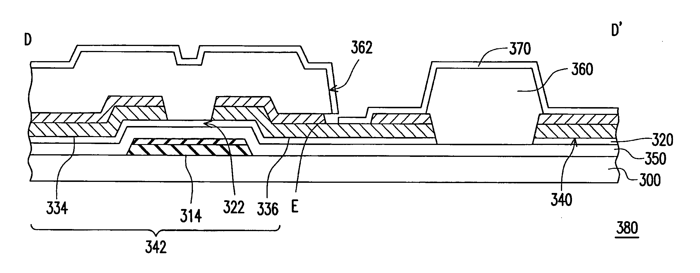
[0059]FIG. 3 is a top view showing the first photomasking process of the active matrix array structure according to a first embodiment of the invention. FIGS. 4A to 4D are cross sectional views of FIG. 3 along the cutting lines AA′, BB′ CC′ and DD″, respectively. Referring to FIGS. 3 and 4A to 4D, the fabrication of an active matrix array structure of this embodiment of the invention includes forming a first conductive layer (not shown) on a substrate 300, and patterning the first conductive layer (not shown) by performing a first photomasking process to form a first patterned conductive layer 310. The first patterned conductive layer 310 includes a plurality of scan lines 312, a plurality of gates 314 and a plurality of scan contact pads 316, and the scan lines 312 are connected with the gates 314 and the scan contact pads 316.
[0060]In this embodiment, the first patterned conductive layer 310 includes, for example, a multi-layer of metal stacked layer structure constructed with a f...
second embodiment
[0081]FIG. 14 is a schematic diagram illustrating an active matrix array structure according to a second embodiment of the present invention. FIGS. 15A to 15D are cross-sectional views of FIG. 14 along the cutting lines AA′, BB′ CC′ and DD′. Referring to FIGS. 14 and 15A to 15D, the active matrix array structure 600 and the active matrix array structure 380 in the first embodiment are substantially similar. The active matrix array structure 600 further includes a patterned passivation layer 680 configured between the patterned overcoat layer 360 and the substrate 300. Moreover, in this embodiment, the metal stacked layer structure that forms the gate 314, the scan line 312 and the scan pad 316 includes, for example, a stacked structure of aluminum and molybdenum or a molybdenum / aluminum / molybdenum three-layered stacked structure. Concurrently, the metal structure that forms the date lines 332, the source electrodes 334, the drain electrodes 336 and the data contact pads 338 includes...
third embodiment
[0085]FIG. 16 is a schematic diagram illustrating an active matrix array structure according to a third embodiment of the present invention. FIGS. 17A to 17D are cross-sectional views of FIG. 16 along the cutting lines AA′, BB′ CC′ and DD′. Referring to FIG. 16 and FIGS. 17A to 17D, a first patterned conductive layer 702 is formed on a substrate 700. The first patterned conductive layer 702 is a stacked layer structure that includes a first aluminum metal layer and a first molybdenum layer. During the first photomasking process, a normal photomask is used to perform photolithograph and etching processes in forming a first patterned conductive layer 702.
[0086]Moreover, the first patterned conductive layer 702 includes a scan line 704, a scan contact pad 706, a gate 708, a capacitor lower electrode 710 and an auxiliary pad 712. The scan line 704, the scan contact pad 706, the gate 708 and the capacitor lower electrode 710 are electrically connected. Moreover, the scan contact pad 706 ...
PUM
 Abstract
Description
Claims
Application Information