Apparatus for and Method of Current Leakage Reduction in Static Random Access Memory Arrays

Inactive Publication Date: 2009-07-09
IBM CORP
View PDF6 Cites 30 Cited by
  • Summary
  • Abstract
  • Description
  • Claims
  • Application Information

AI Technical Summary

Benefits of technology

[0014]The invention is operative to facilitate the development of synthesis tools which generate more efficient SRAM arrays to be incorporated

Problems solved by technology

Higher density manufacturing processes (e.g., 65 and 45 nm) are resulting in greater current leakage.
Therefore, both the increasing quantity of cache memory and the higher density of microprocessor designs are both contributing to an increase in current leakage, even when the microprocessor is not in use.
A problem associated with this memory cell is that after an SRAM cell is precharged, current leakage occurs in the NFET read stack.
In some designs a majority of the microprocessor's power consumption during an active mode is lost to leakage in arrays of SRAM cache memory cell.
For idle microprocessors, SRAM memory array leakage can account for as much as 50% of overall power consumption.
Anoth

Method used


Image

  • Apparatus for and Method of Current Leakage Reduction in Static Random Access Memory Arrays
  • Apparatus for and Method of Current Leakage Reduction in Static Random Access Memory Arrays
  • Apparatus for and Method of Current Leakage Reduction in Static Random Access Memory Arrays

Examples


Embodiment Construction

Notation Used Throughout

[0028]The following notation is used throughout this document.

TermDefinitionSRAMStatic Random Access MemoryNFETN Channel Field Effect TransistorPFETP Channel Field Effect Transistor8T SRAMEight Transistor Static Random Access MemoryLBLLocal Bit LineLECLocal Evaluation CircuitRWLRead Word-LineD1A dynamic nodeGBL_ENGlobal Bit Line Enable

DETAILED DESCRIPTION

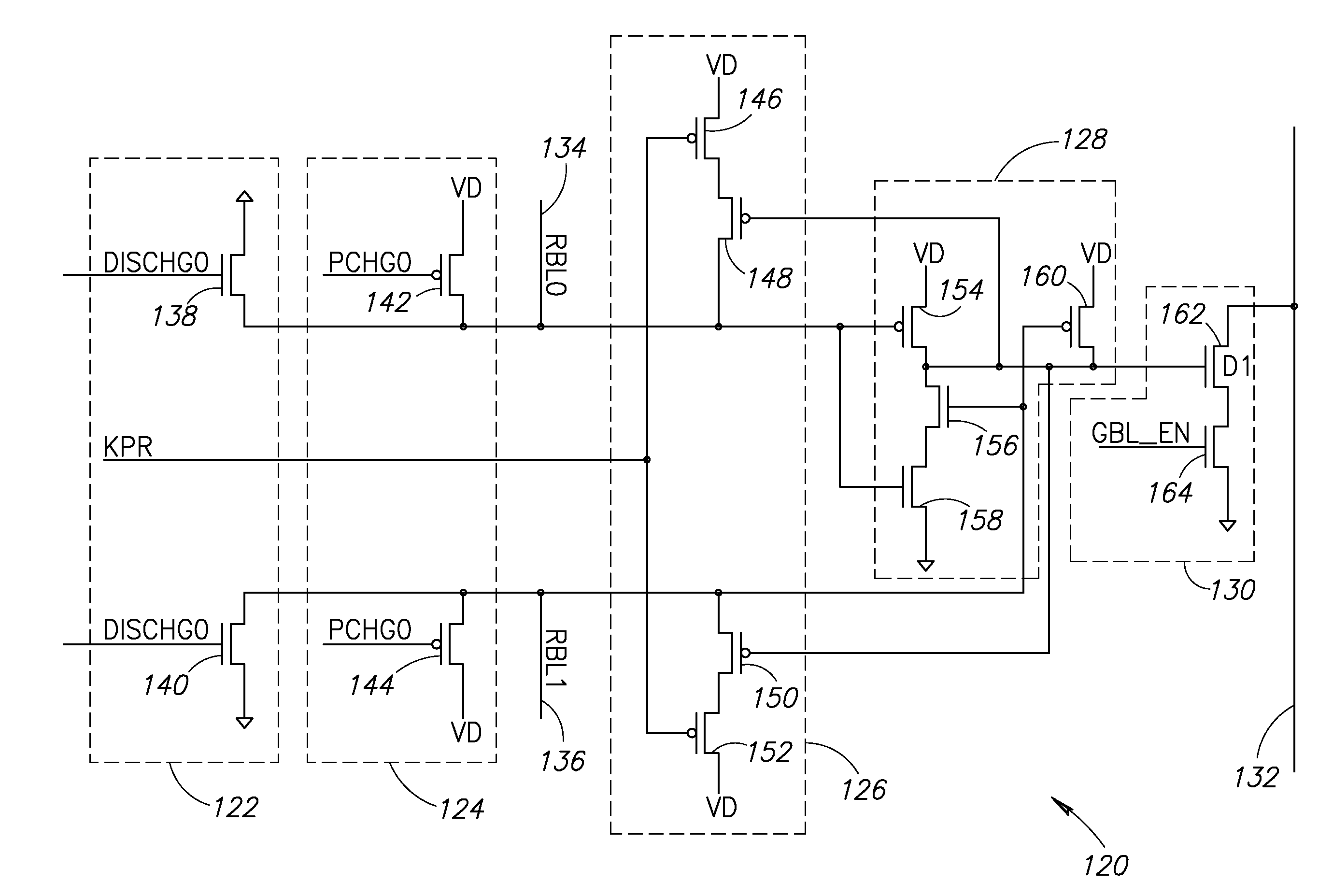
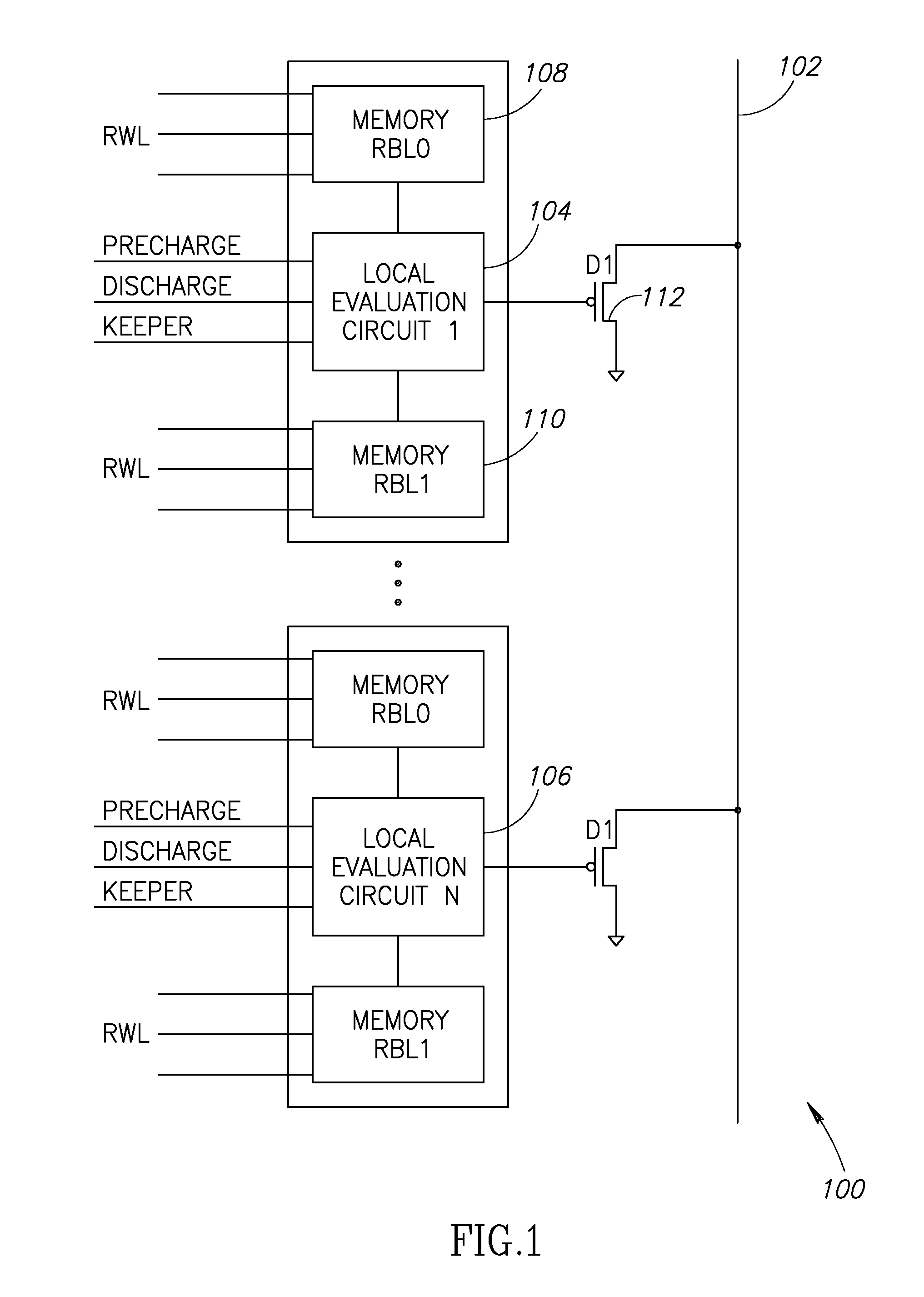
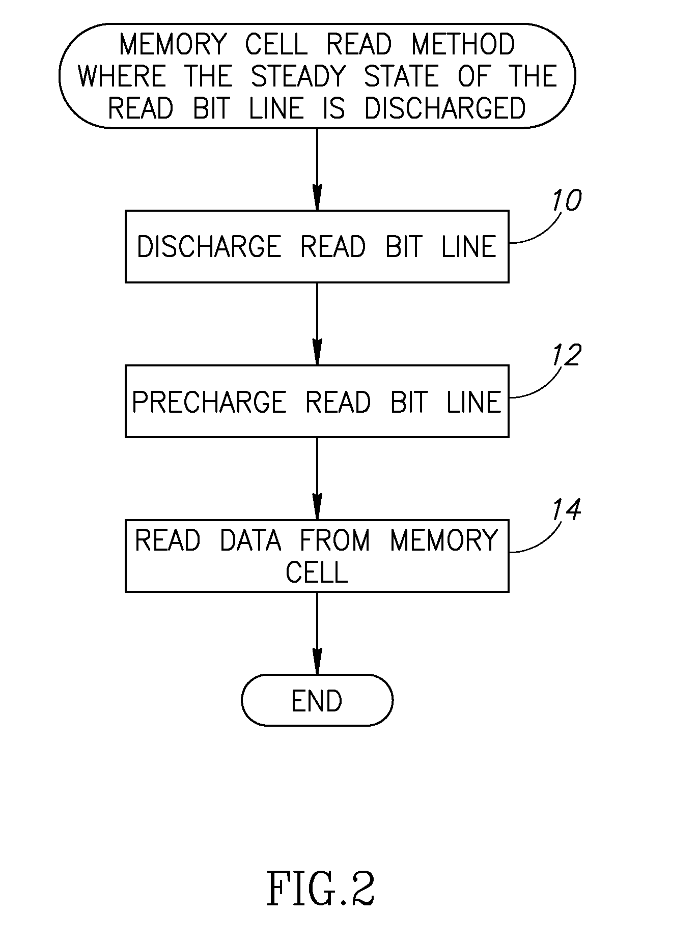
[0029]The present invention is a novel and useful mechanism for reducing current leakage in an SRAM array comprising memory cells that are accessed by an NFET read stack. The current leakage reduction mechanism of the invention enables reading memory cells in a SRAM array whose read bit lines steady state is discharged. The discharged steady state dramatically reduces current leakage and therefore reduces power consumption in the SRAM array.

[0030]The present invention utilizes SRAM memory cells comprise a memory storage circuit and an NFET read stack (also called a pulldown stack). An NFET read stack compri...


PUM


Abstract

A novel and useful mechanism for reducing current leakage in a static random access memory array which significantly reduces the power requirements of the memory array. The method enables the steady state of all local and global bit lines in an SRAM array to be discharged during both active and inactive modes. The memory array consists of memory cells having an N channel field effect transistor read stack. A mechanism is provided to evaluate data from memory cells where the steady state of local and global read bit lines is discharged.

Description

FIELD OF THE INVENTION [0001]The present invention relates to the field of microprocessor design, and more particularly relates to a method of reducing current leakage in static random access memory (SRAM) arrays by enabling the steady state of all local and global bit lines in an SRAM array to be discharged during both active and inactive modes.BACKGROUND OF THE INVENTION [0002]Microprocessor designers are increasingly relying on greater amounts of cache memory in order to increase their performance. In addition, new manufacturing processes, for example, 65 and 45 nanometer (nm) processes are enabling hardware designers to incorporate more cache memory in their designs. Cache memory is extremely fast memory used by the central processing unit to reduce the average time to retrieve data from the most frequently accessed primary memory locations.[0003]Higher density manufacturing processes (e.g., 65 and 45 nm) are resulting in greater current leakage. These manufacturing processes ar...

Claims


Application Information

Patent Timeline
IPC IPC(8): G11C7/00
CPCG11C7/12G11C11/413G11C11/412
Inventor CHRISTENSEN, TODD A.GERHARD, ELIZABETH L.HEYMANN, OMERROZENFELD, AMIRA
Owner IBM CORP
Why Eureka
Try Eureka