Functional device and manufacturing method thereof

Inactive Publication Date: 2009-07-16
SEIKO EPSON CORP
View PDF12 Cites 40 Cited by
  • Summary
  • Abstract
  • Description
  • Claims
  • Application Information

AI Technical Summary

Benefits of technology

[0025]In one aspect of the invention, in the covering step, by the second cover layer being formed in a depressurized space by a vapor growth method, the cavity is depressurized and sealed. By the second cover layer being formed in the depressurized space by the vapor growth method, it is possible to extremely easily depressurize and seal the cavity. However, the inv

Problems solved by technology

This kind of depression of the cover, in some cases, causing a poor operation due to the cover making contact with the MEMS structure, or the like, may result in a reduction in an electronic device manufacturing yield, or a reduction in a product quality.
Furthermore, as an aspect of the cover covering the cavity also varies depending on a difference in thermal expansion caused by a layer structure of the cover, a change in manufacturing conditions, or the like, a deformation, such as the inward depression or an outward protrusion, may

Method used


Image

  • Functional device and manufacturing method thereof
  • Functional device and manufacturing method thereof
  • Functional device and manufacturing method thereof

Examples


Embodiment Construction

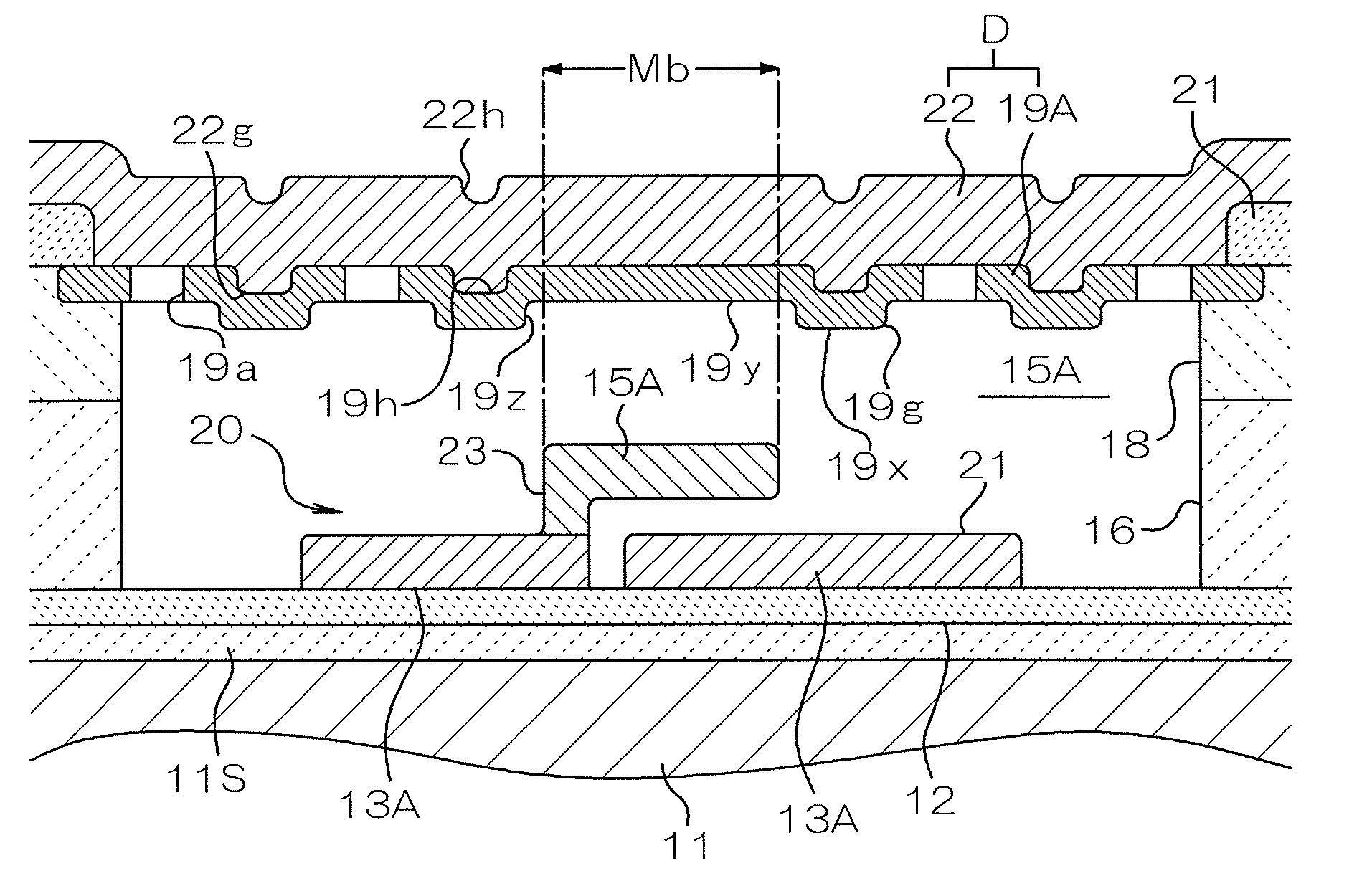
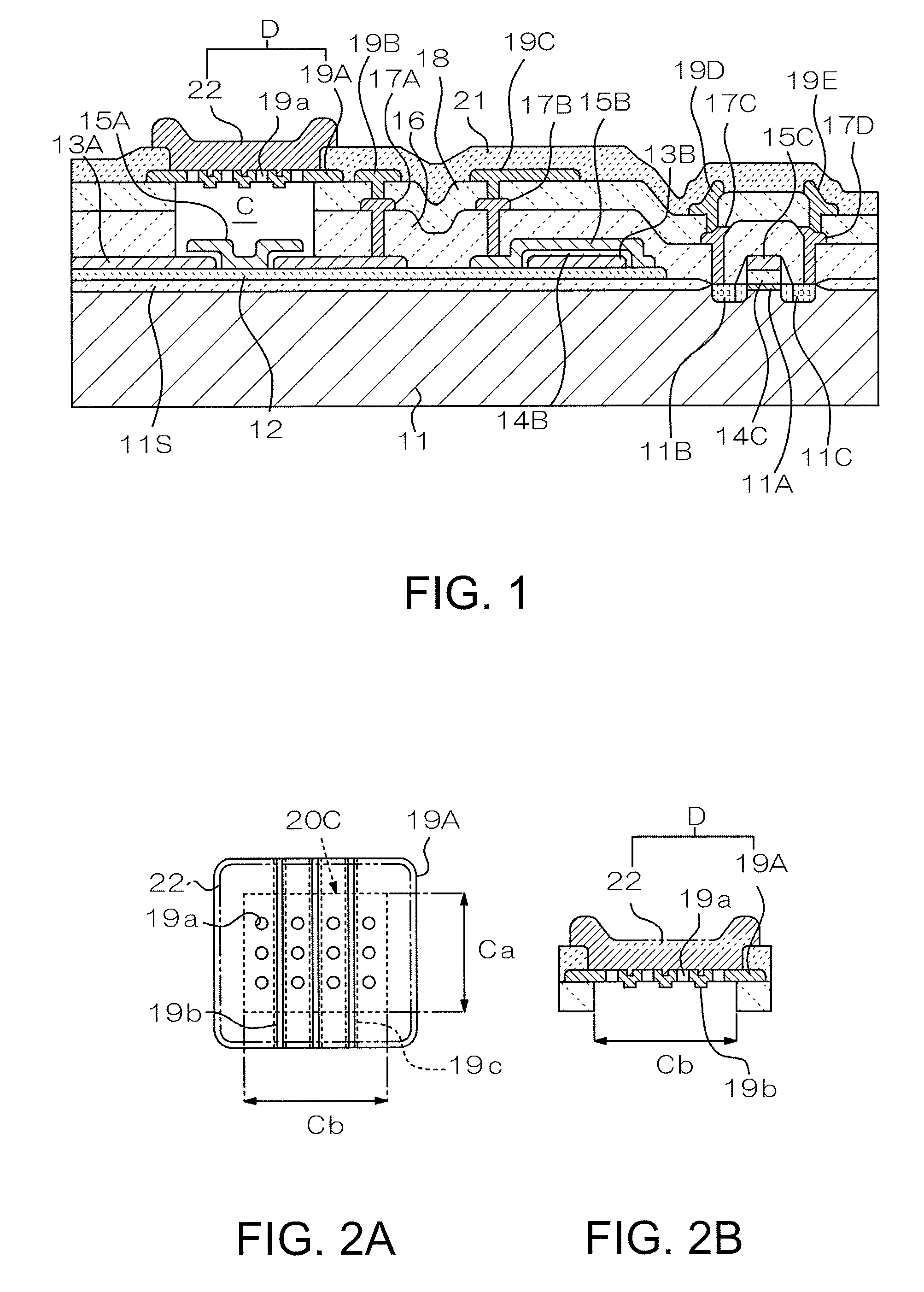
[0045]Next, referring to the accompanying drawings, a detailed description will be given of embodiments of the invention. Firstly, a description will be given of an embodiment of a functional device according to some aspects of the invention. FIGS. 1, 2A and 2B are diagrammatic enlarged vertical sectional views showing an example of a cross-sectional structure of the functional device according to some aspects of the invention.

[0046]In the embodiment, a substrate 11 formed of a semiconductor substrate, such as a silicon or compound semiconductor substrate, or the like, is used. However, in the invention, the substrate 11 may also be configured of another material such as glass, ceramics, a sapphire, a diamond, or a synthetic resin.

[0047]In the embodiment, an element separation film 11S such as a LOCOS (Local Oxidation of Silicon) film is formed on the substrate 11 by an ordinary method (a thermal oxidation method or the like), on top of which is formed a foundation layer (an element...


PUM


Abstract

A functional device includes: a substrate; a functional structure formed on the substrate; a cavity in which the functional structure is disposed; and a cover which covers the cavity, wherein the cover includes a bumpy structure including rib shaped portions, or groove shaped portions, which cross a covering range covering at least the cavity.

Description

BACKGROUND[0001]1. Technical Field[0002]The present invention relates to a functional device and a manufacturing method thereof, and particularly, to a functional device in which a functional structure of an MEMS (microelectromechanical system) or the like is disposed in a cavity configured in a substrate, and a manufacturing method thereof.[0003]2. Related Art[0004]In general, an MEMS (microelectromechanical system) acting as a functional device is manufactured as various electronic parts utilizing a micropatterning technology used in a semiconductor manufacturing process or the like. In many cases, at least one portion of MEMS structures is contained and disposed inside a cavity configured in a substrate, and the cavity is hermetically sealed from above by a cover when necessary, and put into a condition in which it is depressurized and sealed, or a condition in which a specialty gas is sealed in it.[0005]For example, in JP-A-2004-314292, a sealing structure is described which is ...

Claims


Application Information

Patent Timeline
IPC IPC(8): H01L23/02H01L21/50
CPCB81B3/007B81C2203/0163H01L2924/0002H01L2924/00
Inventor INABA, SHOGO
Owner SEIKO EPSON CORP
Why Eureka
Try Eureka