Package structure module with high density electrical connections and method for packaging the same

a technology of electrical connections and packaging structure, which is applied in the field of packaging structure modules and a method for packaging the same, can solve the problems of difficult to reduce in size, complex mechanical mechanism long optical paths of laser printer heads, so as to reduce product size, material cost and manufacturing cost, and increase production speed

Inactive Publication Date: 2009-07-23
UNIVERSAL SCI IND CO LTD
View PDF2 Cites 5 Cited by
  • Summary
  • Abstract
  • Description
  • Claims
  • Application Information

AI Technical Summary

Benefits of technology

[0015]Therefore, the present invention does not need to use a wire-bonding process as in the prior art that requires a long time. Hence, the present invention not only can reduce product size, material cost, and manufacturing cost, but also increases production speed.

Problems solved by technology

However, a laser printer head of the prior art has many optical components, and the mechanism of the laser printer head is complex and the optical path of the laser printer head is very long.
Hence, the optical structure is quite complex and difficult to reduce in size when using a laser as light source.
A highly exact and dense wire bonding process in the foregoing method increases the difficulty of the packaging process.
This reduces the product yield and indirectly raises the manufacturing costs.
Moreover, reducing the volume of the light emitting diodes in order to increase the resolution of the printer, further increases the packaging difficulty.

Method used


Image

  • Package structure module with high density electrical connections and method for packaging the same
  • Package structure module with high density electrical connections and method for packaging the same
  • Package structure module with high density electrical connections and method for packaging the same

Examples


first embodiment

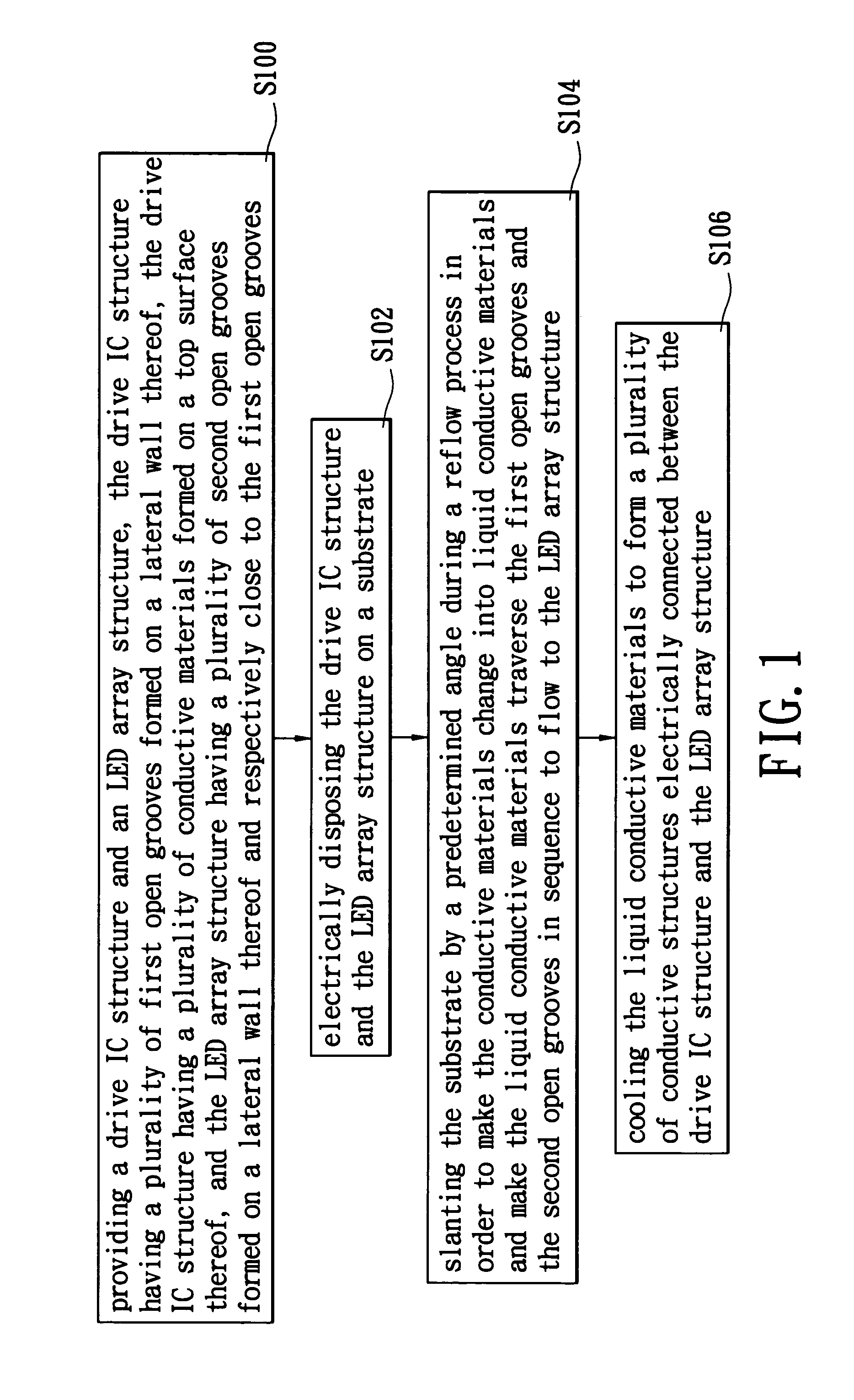
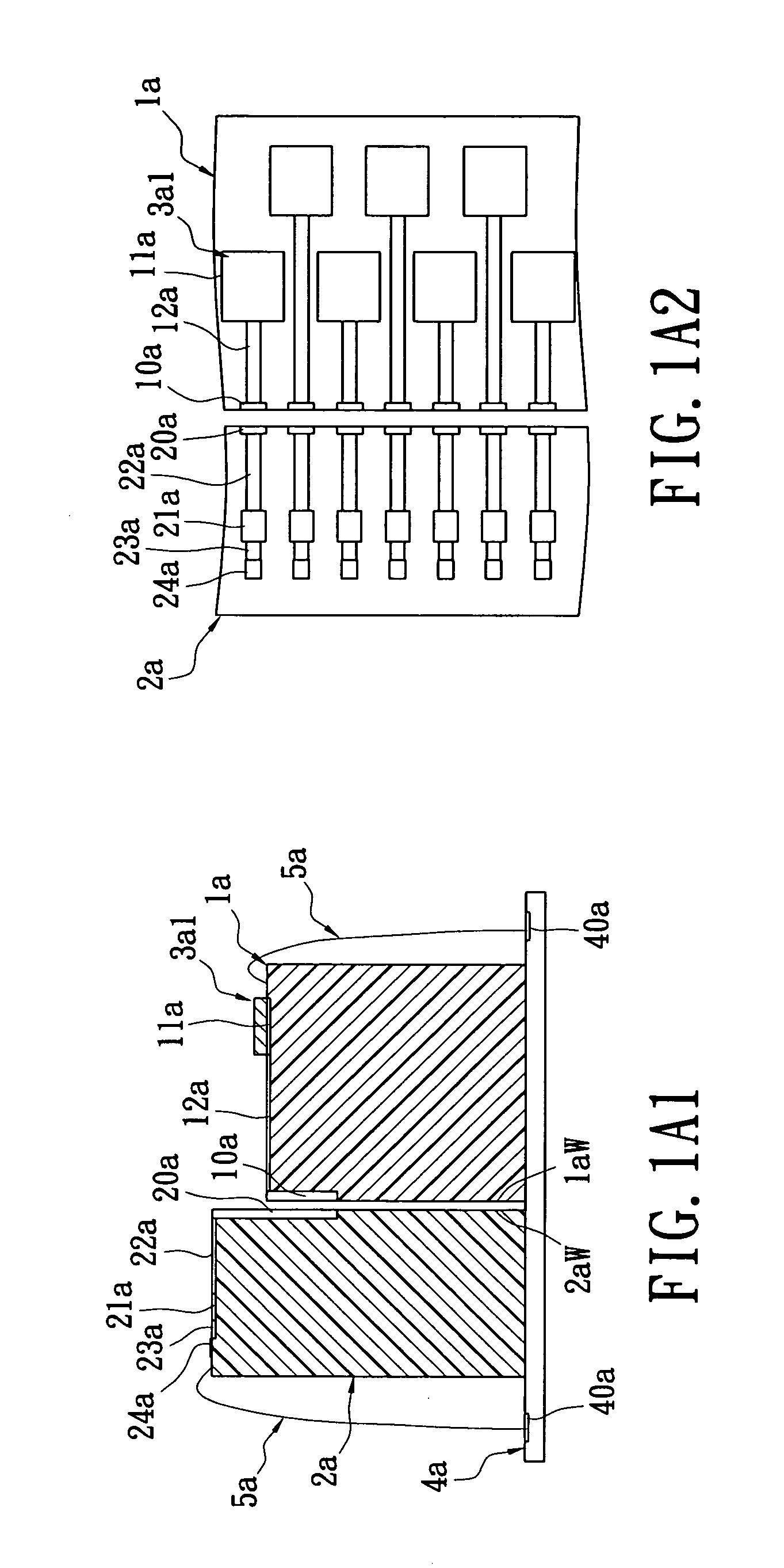
[0027]the present invention provides a method for packaging a package structure module with high density electrical connections. The method includes following steps: referring to FIGS. 1, 1A1 and 1A2 (FIG. 1A2 shows a partial top view of FIG. 1A1), the step of S100 is: providing a drive IC structure 1a (a first structure) and an LED array structure 2a (a second structure), the drive IC structure 1a having a plurality of first open grooves 10a formed on a lateral wall 1aW thereof, the drive IC structure 1a having a plurality of conductive materials 3a1 formed on a top surface thereof, and the LED array structure 2a having a plurality of second open grooves 20a formed on a lateral wall 2aW thereof and respectively close to the first open grooves 10a.

[0028]Moreover, the LED array structure 2a has a height higher than that of the drive IC structure 1a. Each first open groove 10a and each second open grooves 20a are respectively formed on the lateral wall 1aW of the drive IC structure 1...

second embodiment

[0036]the present invention provides a method for packaging a package structure module with high density electrical connections. The method includes following steps: referring to FIGS. 2, 2A1 and 2A2 (FIG. 2A2 shows a partial top view of FIG. 2A1), the step of S200 is: providing a drive IC structure 1b (a first structure) and an LED array structure 2b (a second structure) having an insulation layer 25b formed on a top surface thereof, the drive IC structure 1b having a plurality of first open grooves 10b formed on a lateral wall 1bW thereof, the drive IC structure 1b having a plurality of conductive materials 3b1 formed on a top surface thereof, and the LED array structure 2b having a plurality of second open grooves 20b formed on a lateral wall 2bW thereof and respectively close to the first open grooves 10b.

[0037]Moreover, the LED array structure 2b has a height higher than that of the drive IC structure 1b. Each first open groove 10b and each second open grooves 20b are respecti...

third embodiment

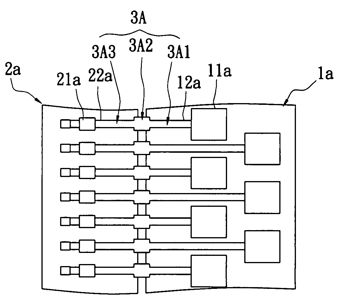
[0046]the present invention provides a method for packaging a package structure module with high density electrical connections. The method includes following steps: referring to FIGS. 3, 3A1 and 3A2 (FIG. 3A2 shows a partial top view of FIG. 3A1), the step of S300 is: providing a drive IC structure 1c (a second structure) and an LED array structure 2c (a first structure), the drive IC structure 1c having a plurality of first open grooves 10c formed on a lateral wall 1cW thereof, the LED array structure 2c having a plurality of second open grooves 20c formed on a lateral wall 2cW thereof and respectively close to the first open grooves 10c, and the LED array structure 2c having a plurality of conductive materials 3c1 formed on a top surface thereof.

[0047]Moreover, the drive IC structure 1c has a height higher than that of the LED array structure 2c. Each first open groove 10c and each second open grooves 20c are respectively formed on the lateral wall 1cW of the drive IC structure 1...


PUM


Abstract

A package structure module with high density electrical connections includes a drive IC structure, an LED array structure, and a plurality of conductive structures. The drive IC structure has a plurality of first open grooves formed on a lateral wall thereof. The LED array structure has a plurality of second open grooves formed on a lateral wall thereof to respectively face the first open grooves. Each conductive structure traverse the corresponding first open groove and the corresponding second open groove in order to electrically connect between the drive IC structure and the LED array structure.

Description

BACKGROUND OF THE INVENTION[0001]1. Field of the Invention[0002]The present invention relates to a package structure module and a method for packaging the same, and particularly relates to a package structure module with high density electrical connections and a method for packaging the same.[0003]2. Description of the Related Art[0004]In the typical printer technology, a laser is used as a light source in a printer head to scan and transfer the printing information as light signals to a rotating drum in order to generate electrostatic latent images formed on the rotating drum. Moreover, the printing method further includes a toner absorbing step, a transferring step, a hot pressing step, an electrostatic discharging step etc. to reach printing. However, a laser printer head of the prior art has many optical components, and the mechanism of the laser printer head is complex and the optical path of the laser printer head is very long. Hence, the optical structure is quite complex and...

Claims


Application Information

Patent Timeline
Patent Type & Authority Applications(United States)
IPC IPC(8): H01L33/00
CPCB41J2/45H01L24/73H01L2924/12041H01L24/24H05K2203/1527H01L25/167H01L27/153H05K1/142H05K3/3405H05K3/3442H05K3/36H01L2224/48091H01L2924/00014H01L2924/00H01L2924/14
Inventor WU, MING-CHE
Owner UNIVERSAL SCI IND CO LTD
Why Eureka
Try Eureka