Post bump and method of forming the same

Inactive Publication Date: 2009-07-23
SAMSUNG ELECTRO MECHANICS CO LTD
View PDF1 Cites 20 Cited by
  • Summary
  • Abstract
  • Description
  • Claims
  • Application Information

AI Technical Summary

Benefits of technology

[0011]An aspect of the invention provides a post bump and a method of forming the post bump, which prevent deviations i

Problems solved by technology

Because of this trend, however, flip chip packaging is liable to provide lower reliability in the bump connections between a circuit board and a semiconductor chip.
With this method of forming post bumps according to the related art, however, the operation of filling the remaining parts of the apertures 110 with solder 114 can result in uneven amounts of plating, due to the potential differenc

Method used


Image

  • Post bump and method of forming the same
  • Post bump and method of forming the same
  • Post bump and method of forming the same

Examples


Embodiment Construction

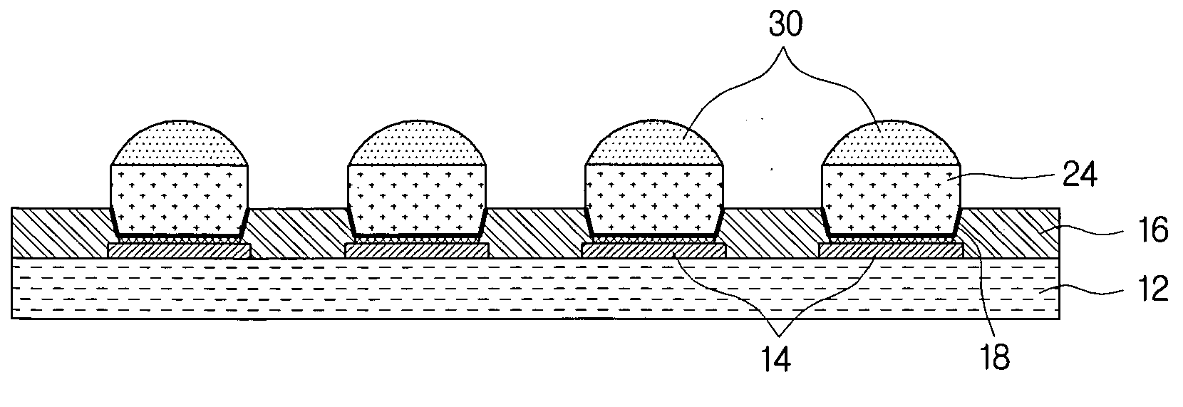
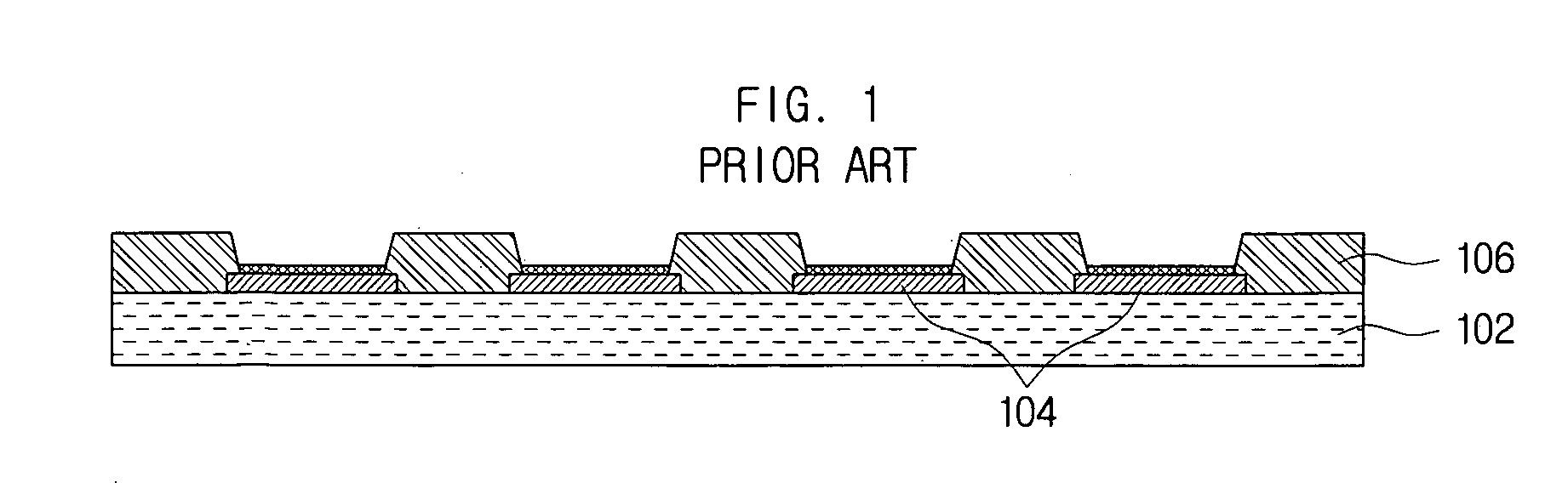
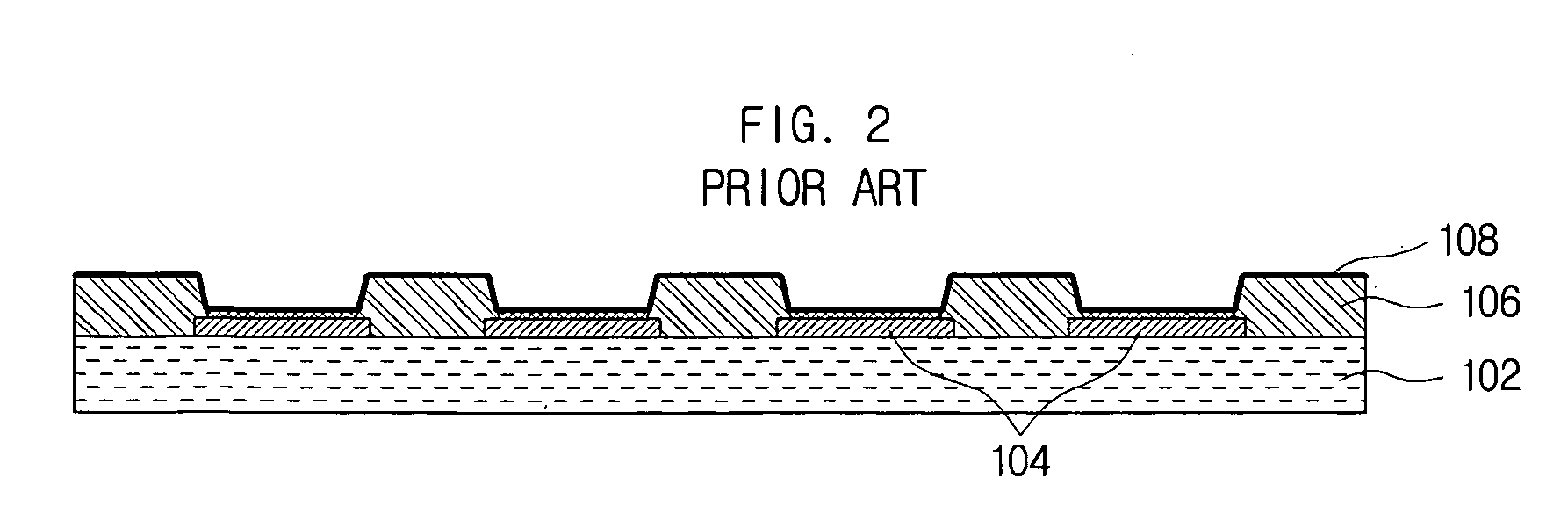
[0033]As the invention allows for various changes and numerous embodiments, particular embodiments will be illustrated in the drawings and described in detail in the written description. However, this is not intended to limit the present invention to particular modes of practice, and it is to be appreciated that all changes, equivalents, and substitutes that do not depart from the spirit and technical scope of the present invention are encompassed in the present invention. In the description of the present invention, certain detailed explanations of related art are omitted when it is deemed that they may unnecessarily obscure the essence of the invention.

[0034]The terms used in the present specification are merely used to describe particular embodiments, and are not intended to limit the present invention. An expression used in the singular encompasses the expression of the plural, unless it has a clearly different meaning in the context. In the present specification, it is to be un...


PUM

PropertyMeasurementUnit
Electrical resistanceaaaaaaaaaa
Electrical conductoraaaaaaaaaa
Areaaaaaaaaaaa

Abstract

A post bump and a method of forming the post bump are disclosed. The method of forming the post bump can include: forming a resist layer, in which an aperture is formed in correspondence to a position of an electrode pad, over a substrate, on which the electrode pad is formed; forming a metal post by filling a part of the aperture with a metallic material; filling a remaining part of the aperture with solder; reflowing the solder by applying heat; and removing the resist layer. This method can be utilized to prevent deviations in the plated solder and prevent the unnecessary flowing of the solder over the sides of the metal post during reflowing, so that the amount of solder used can be minimized.

Description

CROSS-REFERENCE TO RELATED APPLICATIONS[0001]This application claims the benefit of Korean Patent Application No. 10-2008-0006487 filed with the Korean Intellectual Property Office on Jan. 22, 2008, the disclosure of which is incorporated herein by reference in its entirety.BACKGROUND[0002]1. Technical Field[0003]The present invention relates to a post bump and a method of forming the post bump.[0004]2. Description of the Related Art[0005]Flip chip packaging is a technique of bonding and packaging an electronic component in a circuit board, where the component, such as a semiconductor chip, and the circuit board are attached by fusing solder bumps onto the semiconductor chip or the circuit board, instead of using additional connection structures such as wires.[0006]In accordance with current requirements for high-speed, high-capacity data processing, as well as for smaller, lighter, and thinner electronic products, components are trending towards smaller bump pitch. Because of this ...

Claims


Application Information

Patent Timeline
IPC IPC(8): H01L23/488H01L21/44H05K3/00H05K1/00
CPCH01L21/4853Y10T29/49155H01L24/02H01L24/03H01L24/11H01L24/12H01L24/16H01L2224/0401H01L2224/1147H01L2224/11901H01L2224/13022H01L2224/1308H01L2224/13082H01L2224/13111H01L2224/13147H01L2224/16H01L2924/01004H01L2924/01029H01L2924/01047H01L2924/0105H01L2924/01078H01L2924/01082H01L2924/014H01L2924/30105H01L2924/3025H05K3/243H05K3/3484H05K3/4007H05K2201/0367H05K2203/043H05K2203/054H05K2203/0568H05K2203/0571H01L23/49816H01L2224/1131H01L2924/01033H01L2924/01006H01L2924/01005H01L2924/00013H01L2924/00014H01L2224/13099H01L2224/29099H01L24/05H01L24/13H01L2224/119H01L2224/13013H01L2224/13014H01L2224/81193H05K3/3485H01L2224/11849
Inventor CHOI, JIN-WONRYU, CHANG-SUPCHO, SEUNG-HYUNKIM, SEUNG-WAN
Owner SAMSUNG ELECTRO MECHANICS CO LTD
Why Eureka
Try Eureka