Method of performing lithographic processes

a technology of lithographic process and overlay accuracy, applied in photomechanical treatment, instruments, electrical equipment, etc., can solve the problems of poor overlay accuracy, failure of formed electric circuit, and defects in the structure of mos transistor b, so as to improve the overlay accuracy and the performing efficiency of lithographic process.

Inactive Publication Date: 2009-07-30
UNITED MICROELECTRONICS CORP
View PDF2 Cites 5 Cited by
  • Summary
  • Abstract
  • Description
  • Claims
  • Application Information

AI Technical Summary

Benefits of technology

[0010]It is therefore the primary object of the present invention to provide a method of performing lithographic processes on a wafer in a lithographic apparatus having multiple stages so to improve the overlay accuracy and the performing efficiency of the lithographic processes.

Problems solved by technology

Otherwise, the electric circuit pattern in one material layer may not cooperate with the underlying electric circuit pattern, and the formed electric circuit therefore fails.
Therefore, if there is a serious bias of the overlay accuracy due to the lithographic apparatus, defects usually occur in the structure of the MOS transistor 20.
As shown in FIG. 2, the contact plugs 36 are not disposed in the predetermined positions in practice due to a poor overlay accuracy of the lithographic process during the manufacture of the contact plugs 36.
However, with the shrinking dimensions of integrated circuits, strict overlay accuracy is required as well.
It is still a significant issue to improve the overlay accuracy and the performing efficiency of the lithographic processes.

Method used


Image

  • Method of performing lithographic processes
  • Method of performing lithographic processes
  • Method of performing lithographic processes

Examples


Embodiment Construction

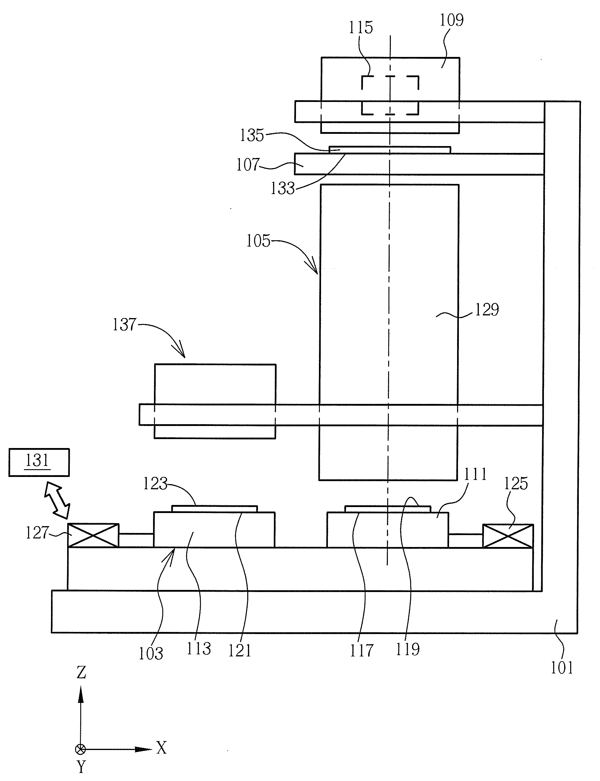
[0024]For clarity of illustration, a lithographic apparatus having multiple stages applied to the method of the present invention is first described. Please refer to FIG. 3, which is a schematic diagram illustrating a lithographic apparatus having multiple stages and the related operation, where like number numerals designate similar or the same parts, regions or elements. As FIG. 3 diagrammatically shows, the lithographic apparatus 100 is provided with a frame 101 that supports in that order, a positioning device 103, a projection system 105, an orientation system 137, a mask holder 107, and a radiation source 109. The positioning device 103 includes a first wafer chuck 111 and a second wafer chuck 113. The lithographic apparatus 100 shown in FIG. 3 can be an optical lithographic apparatus whose radiation source 109 includes a light source 115. The first wafer chuck 111 includes a support surface 117, which extends perpendicularly to the Z-direction and on which a first wafer 119 c...


PUM


Abstract

Method of performing lithographic processes on a wafer in a lithographic apparatus having multiple stages. First, a lithographic apparatus including a first wafer chuck and a second wafer chuck is provided. Subsequently, a cassette including a plurality of wafers is provided in the lithographic apparatus, and each wafer has a wafer identification. Thereafter, the first wafer chuck is set for holding the wafers having odd wafer identifications, and the second wafer chuck is set for holding the wafers having even wafer identifications. Next, a first lithographic process is performed on each wafer by the lithographic apparatus.

Description

BACKGROUND OF THE INVENTION[0001]1. Field of the Invention[0002]The present invention relates to a method of performing lithographic processes, and more particularly, to a method of performing lithographic processes on a wafer in a lithographic apparatus having multiple stages.[0003]2. Description of the Prior Art[0004]Lithographic technologies are key technologies to affect the critical dimensions in the semiconductor processes; and overlay accuracies are key factors to control the lithographic technology. Most of electric circuit patterns are formed by transferring the patterns of masks to photoresists in the lithographic processes, and thereafter transferring the patterns of photoresists to the material layers of a wafer in the etching processes. Thus, the patterns of masks must be disposed in exact positions in every etching process for forming electric circuit patterns in each material layer. Otherwise, the electric circuit pattern in one material layer may not cooperate with t...

Claims


Application Information

Patent Timeline
Patent Type & Authority Applications(United States)
IPC IPC(8): H01L21/02
CPCG03F7/70733G03F7/70541
Inventor HUANG, CHI-CHINGYEN, TZU-CHINGLO, SHIH-CHIEHWU, WEN-TSUNG
Owner UNITED MICROELECTRONICS CORP
Why Eureka
Try Eureka