Device mounting board and manufacturing method therefor, and semiconductor module

a technology of mounting board and semiconductor module, which is applied in the direction of etching metal masks, transportation and packaging, nuclear engineering, etc., can solve the problems of increasing i/o count, generating demand for smaller and thinner packages, and liable to be separated or peeled off from the insulating film in the through-hole, so as to improve the adhesion and improve the connection reliability

Inactive Publication Date: 2009-08-06
SANYO ELECTRIC CO LTD
View PDF50 Cites 27 Cited by
  • Summary
  • Abstract
  • Description
  • Claims
  • Application Information

AI Technical Summary

Benefits of technology

[0008]The present invention has been made in view of the foregoing circumstances, and a general purpose thereof is to provide a technology for improving the adhesion between a via conductor,

Problems solved by technology

Thus the higher integration of LSI chips is causing increases in I/O count, which in turn generates demand for smaller and thinner packages.
In the conventional device mounting board, the via conductor formed in the through-hole is a thin film having the thickness of about 10 μm, so that there is a problem that the via conductor is liable to be separated or pealed off from

Method used


Image

  • Device mounting board and manufacturing method therefor, and semiconductor module
  • Device mounting board and manufacturing method therefor, and semiconductor module
  • Device mounting board and manufacturing method therefor, and semiconductor module

Examples


first embodiment

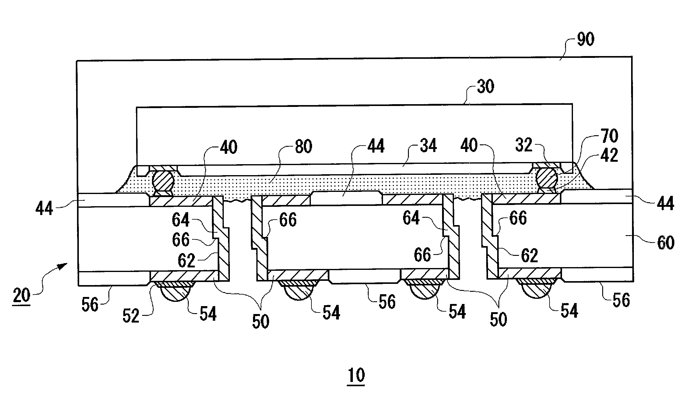
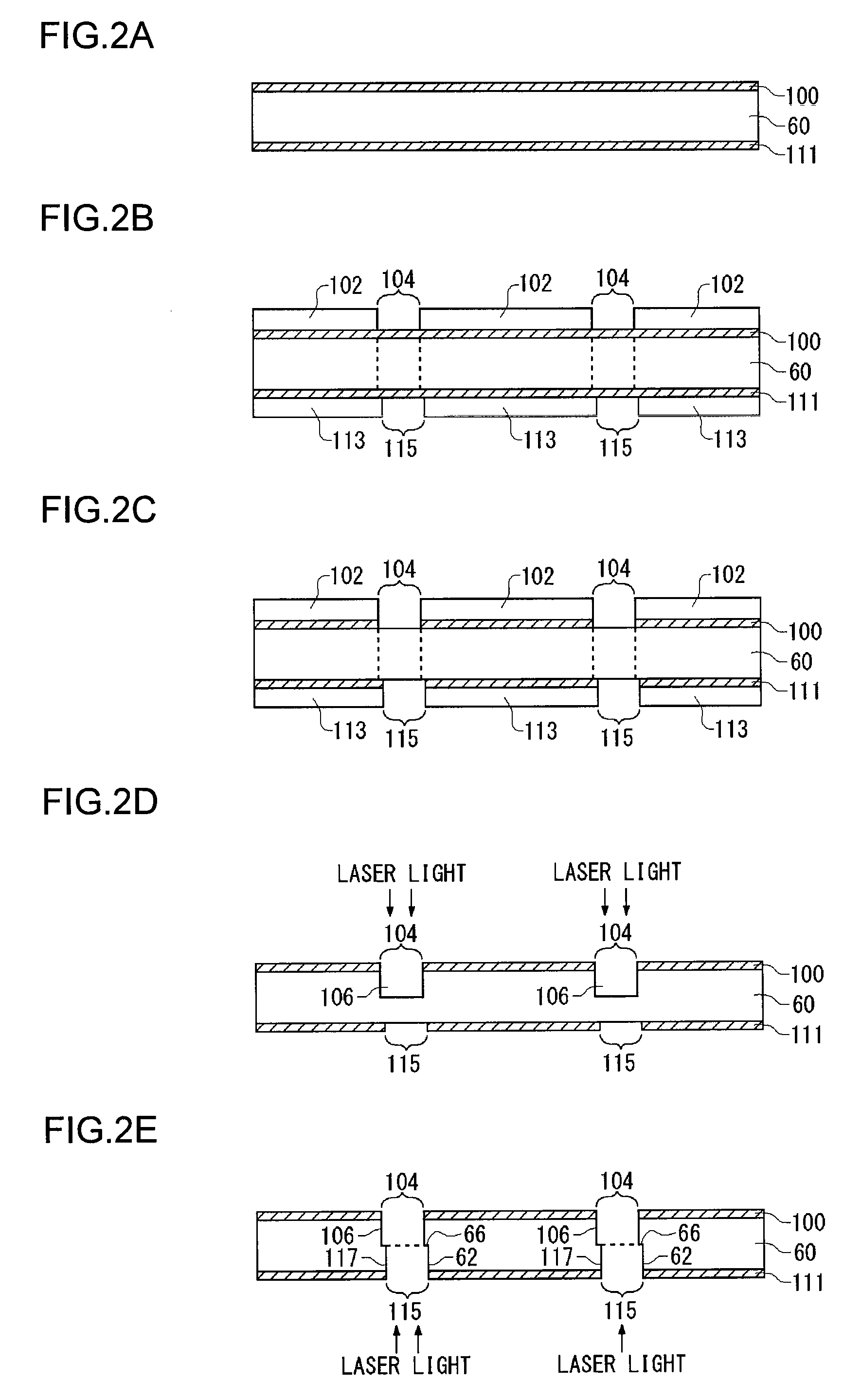
[0039]FIG. 1 is a cross-sectional view showing a structure of a semiconductor module 10 according to a first embodiment of the present invention. The semiconductor module 10 has a packaged structure where a semiconductor device 30 is mounted on a device mounting board 20.

[0040]The device mounting board 20 has a double-layer wiring structure where a first wiring layer 40 and a second wiring layer 50 are stacked through the medium of an insulating layer 60 held therebetween. The first wiring 40 and the second wiring layer 50 are each formed of metal with satisfactory electric conductivity. The device mounting board 20, which does not have a supporting substrate, is of thin type and can achieve high-density packaging of semiconductor devices and the like. Such a structure is achieved by Integrated System in Board or ISB (registered trademark) developed by the applicant of this patent specification. The detailed description thereof is given in Japanese Patent Application Laid-Open No. 2...

second embodiment

[0062]FIG. 5 is a cross-sectional view showing a structure of a semiconductor module 10 according to a second embodiment of the present invention. Similar to the first embodiment, the semiconductor module 10 according to the second embodiment has a packaged structure where a semiconductor device 30 is mounted on a device mounting board 20. The same components as those of the first embodiment are given the same reference numerals and the explanation thereof is omitted as appropriate, and a description will be given here of the semiconductor module 10 according to the second embodiment centering around a structure different from that of the first embodiment.

[0063]In the semiconductor module 10 according to the second embodiment, a solder resist layer 44 is formed over the entire surface of a device mounting board 20 except for the mounting region of solder balls 70. In other words, the solder balls 70 are mounted on electrode pads 42 in openings of the solder resist layer 44 formed ov...

third embodiment

[0068]FIG. 6 is a cross-sectional view showing a structure of a semiconductor module 10 according to a third embodiment of the present invention. Similar to the first embodiment, the semiconductor module 10 according to the third embodiment has a packaged structure where a semiconductor device 30 is mounted on a device mounting board 20. The same components as those of the first embodiment are given the same reference numerals and the explanation thereof is omitted as appropriate, and a description will be given here of the semiconductor module 10 according to the third embodiment centering around a structure different from that of the first embodiment.

[0069]In the semiconductor module 10 according to the third embodiment, a solder resist layer 44 is formed over the entire upper surface of a device mounting board 20 except for the underneath of the mounting region of the semiconductor device 30 and the mounting region of solder balls 70. In the underneath of the semiconductor device...


PUM


Abstract

A device mounting board has a double-layer wiring structure where a first wiring layer and a second wiring layer are stacked together with an insulating layer held between the first and second wiring layers. The first wiring layer and the second wiring layer are electrically connected by way of a via conductor provided on a side wall of a through-hole that penetrates the insulating layer. The through-hole that penetrates the insulating layer has a stepped portion. The via conductor, provided along the insulating layer in the via conductor, has a step associated with the stepped portion of the via conductor.

Description

CROSS-REFERENCE TO RELATED APPLICATIONS[0001]This application is based upon and claims the benefit of priority from the prior Japanese Patent Application No. 2008-022061, filed on Jan. 31, 2008, and Japanese Patent Application No. 2009-011616, filed on Jan. 22, 2009, the entire contents of which are incorporated herein by reference, the entire contents of which are incorporated herein by reference.BACKGROUND OF THE INVENTION[0002]1. Field of the Invention[0003]The present invention relates to a device mounting board and a manufacturing method therefor, a semiconductor module and a portable device including the same.[0004]2. Description of the Related Art[0005]Portable electronic devices, such as mobile phones, PDAs, DVCs, and DSCs, are today gaining an increasing variety of functions. And to be accepted by the market, they have to be smaller in size and lighter in weight, and in order to achieve this there is a growing demand for highly-integrated system LSIs. On the other hand, the...

Claims


Application Information

Patent Timeline
IPC IPC(8): H05K1/16B05D3/06H05K1/11
CPCH05K1/114H01L2924/15151H05K3/0032H05K3/427H05K2201/09563H05K2201/09845H05K2203/0554H05K2203/1572H01L2224/16225H01L2224/32225H01L2224/73204H01L2924/15311H05K1/115H01L2924/00H01L2224/05571H01L2224/05573H01L2924/00014H01L2224/05599
Inventor USUI, RYOSUKENAKAMURA, TAKESHIKUZUU, TOMOHIROIGARASHI, YUSUKE
Owner SANYO ELECTRIC CO LTD
Why Eureka
Try Eureka