Timing Signal Generating Circuit, Semiconductor Integrated Circuit Device and Semiconductor Integrated Circuit System to which the Timing Signal Generating Circuit is Applied, and Signal Transmission System

a timing signal and generating circuit technology, applied in the direction of generating/distributing signals, pulse techniques, instruments, etc., can solve the problems of speed gap becoming a bottleneck in boosting computer performance, signal transmission between chips, and speed of signal transmission between devices and between constituent circuits within one lsi chip (semiconductor integrated circuit devices), and achieves simple circuitry, high accuracy, and high adjustment accuracy

Inactive Publication Date: 2009-08-06
FUJITSU LTD
View PDF35 Cites 109 Cited by
  • Summary
  • Abstract
  • Description
  • Claims
  • Application Information

AI Technical Summary

Benefits of technology

[0011]An object of a first aspect of the present invention is to provide a semiconductor integrated circuit device that permits timing design with relatively high adjustment accuracy to be done in a short period. An object of a second aspect of the present invention is to provide a signal transmission system capable of high-speed, error-free signal transmission without being affected by skew on each signal line. An object of a third aspect of the present invention is to provide a timing signal generating circuit that can generate with simple circuitry and with high accuracy a plurality of timing signals, having prescribed phase differences, synchronous with a reference clock.
[0021]Further, according to the present invention, there is provided a signal transmission system for transmitting and receiving signals using a plurality of signal lines, comprising a timing adjusting unit for adjusting the amount of signal delay caused during the transmission and reception of the signals in accordance with skew on each of the signal lines, thereby adjusting signal latch timing at a receiving circuit provided for each of the signal lines so that the latch timing becomes optimum for the signal line.

Problems solved by technology

However, the improvement in DRAM speed has not been so dramatic as the increase in storage capacity, as a result of which a gap between the speed of DRAMs and that of processors has widened and, in recent years, this speed gap has been becoming a bottleneck in boosting computer performance.
Further, with increasing chip size, not only signal transmission between the chips but also the speed of signal transmission between devices and between constituent circuits (circuit blocks) within one LSI chip (semiconductor integrated circuit device) is becoming a major limiting factor in chip performance.

Method used


Image

  • Timing Signal Generating Circuit, Semiconductor Integrated Circuit Device and Semiconductor Integrated Circuit System to which the Timing Signal Generating Circuit is Applied, and Signal Transmission System
  • Timing Signal Generating Circuit, Semiconductor Integrated Circuit Device and Semiconductor Integrated Circuit System to which the Timing Signal Generating Circuit is Applied, and Signal Transmission System
  • Timing Signal Generating Circuit, Semiconductor Integrated Circuit Device and Semiconductor Integrated Circuit System to which the Timing Signal Generating Circuit is Applied, and Signal Transmission System

Examples


first embodiment

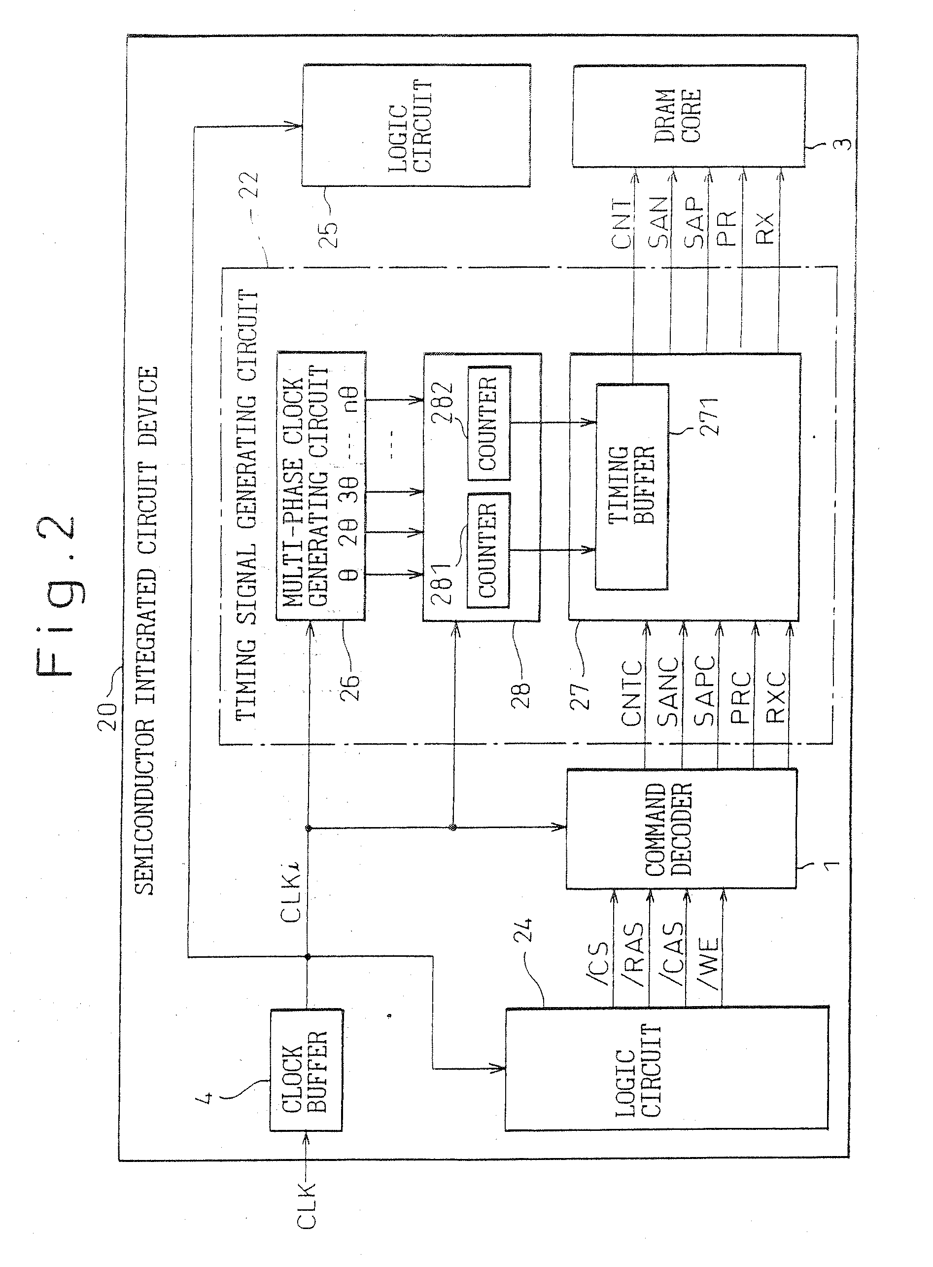
[0147]FIG. 2 is a block diagram showing in schematic form a semiconductor integrated circuit device 20 as a first embodiment according to the first aspect of the present invention. The same parts as those in FIG. 1 are designated by the same reference numerals.

[0148]As shown in FIG. 2, the semiconductor integrated circuit device 20 is an ASIC containing: a DRAM comprising a command decoder 1, a DRAM core 3, a clock buffer circuit 4, and a timing signal generating circuit 22; a logic circuit 24 such as a CPU or memory controller; and other logic circuits 25.

[0149]The logic circuits 24 and 25 operate synchronously with the clock CLKi. The logic circuit 24 supplies a chip select signal / CS, a row address strobe signal / RAS, a column address strobe signal / CAS, and a write enable signal / WE to the command decoder 1, and a command appropriate to the combination of the logic values of these signals at the rising of the clock CLKi, for example, is issued from the command decoder 1. The com...

second embodiment

[0159]FIG. 5 is a block circuit diagram showing a portion of the timing signal generating circuit as a second embodiment according to the first aspect of the present invention.

[0160]In the foregoing first embodiment according to the first aspect of the present invention, the bit length must be made long enough that the contents of the loop counters 281 and 282 do not make a complete cycle around the loop within a RAS cycle that starts at the fall of the row address strobe signal / RAS and ends at the next fall thereof.

[0161]In view of this, in the counter circuit 28A of the second embodiment, as shown in FIG. 5, the loop counter 281 counts the clock CLKi, and the clock φ3 and a predetermined bit output of the loop counter 281 are supplied to an AND gate 37 to create the activation timing signal CNT1, while the clock φ4 and a predetermined bit output of the loop counter 281 are supplied to an AND gate 38 to create the deactivation timing signal CNT2.

[0162]By so doing, the outputs of t...

third embodiment

[0163]FIG. 6 is a block circuit diagram showing a portion of the timing signal generating circuit 22 as a third embodiment according to the first aspect of the present invention.

[0164]As shown in FIG. 6, in the circuit of the third embodiment, the AND gate 36 in FIG. 5 is eliminated and, instead, an AND gate 283 is used in the counter circuit 28B, and the clock CLKi and the control command CNTC are supplied to the AND gate 283 whose output is then counted by the loop counter 281.

[0165]According to this configuration, the output of the flip-flop 30 can be used directly as the control signal CNT, and there is no need to consider the delay associated with the AND gate 36 in FIG. 5. Furthermore, since the CLKi is passed through the AND gate 283 and counted by the loop counter 281 only when the control command CNTC is at a high level “H”, the power consumption of the counter circuit 28B can be reduced.

[0166]Further, the pMOS transistors 33A and 33B and nMOS transistor 35 in FIG. 5 are re...


PUM


Abstract

A semiconductor integrated circuit device has a command decoder for issuing a control command in accordance with a supplied control signal, a DRAM core, and a timing adjusting circuit for supplying the control command, set active for a predetermined period, as a DRAM control signal to the DRAM core. The timing adjusting circuit generates n different clocks that are respectively shifted in phase with respect to a supplied reference clock, and generates the DRAM control signal by setting the control command active in a prescribed operation cycle for only a period starting at a first predetermined clock pulse of a first clock of the n clocks and ending at a second predetermined clock pulse of a second clock of the n clocks. In this way, timing design with relatively high accuracy of adjustment can be done in a short period.

Description

BACKGROUND OF THE INVENTION[0001]1. Field of the Invention[0002]The present invention relates to a timing signal generating circuits a semiconductor integrated circuit device and semiconductor integrated circuit system to which the timing signal generating circuit is applied and a signal transmission system and, more particularly, to a timing signal generating circuit aimed at increasing the speed of signal transmission between LSI (Large Scale Integration Circuit) chips or between a plurality of devices or circuit blocks within one chip.[0003]2. Description of the Related Art[0004]Recently, the performance of components used in computers and other information processing apparatuses has improved rapidly; in particular, the performance of dynamic random access memories (DRAMs) and processors has improved dramatically year by year.[0005]Namely, processor performance has increased dramatically in terms of speeds whereas DRAM performance improvements have been dramatic primarily in term...

Claims


Application Information

Patent Timeline
Patent Type & Authority Applications(United States)
IPC IPC(8): H03L7/00G11C7/10G11C11/407G11C7/22G11C8/18G11C11/4076
CPCG11C7/1072G11C7/22G11C7/222H04L7/0337G11C11/4076H03K2005/00052H04L7/0025G11C8/18G11C11/407
Inventor TAMURA, HIROTAKAYAMAGUCHI, HISAKATSUWAKAYAMA, SHIGETOSHIGOTOH, KOHTAROHOGAWA, JUNJI
Owner FUJITSU LTD
Why Eureka
Try Eureka