Active Array Substrate, Liquid Crystal Display Panel, and Manufacturing Method Thereof

a technology of liquid crystal display panel and active array substrate, which is applied in the direction of instruments, non-linear optics, optics, etc., can solve the problems of polluting the environment, wasting most color resists, and expensive methods, so as to reduce process steps, increase panel efficiency, and reduce costs

Inactive Publication Date: 2009-08-06
AU OPTRONICS CORP
View PDF9 Cites 8 Cited by
  • Summary
  • Abstract
  • Description
  • Claims
  • Application Information

AI Technical Summary

Benefits of technology

[0012]The present invention is directed to a method for manufacturing an active array substrate to increase the efficiency of the panel and decrease costs.
[0013]The present invention is directed to a method for manufacturing an active array substrate. The photoresist in the earlier steps of the process is se

Problems solved by technology

Because the color resists layers are formed by dropping the color resist liquid on the substrate and then performing spin coating, most color resists are wasted when conducting the spin coating pr

Method used


Image

  • Active Array Substrate, Liquid Crystal Display Panel, and Manufacturing Method Thereof
  • Active Array Substrate, Liquid Crystal Display Panel, and Manufacturing Method Thereof
  • Active Array Substrate, Liquid Crystal Display Panel, and Manufacturing Method Thereof

Examples


first embodiment

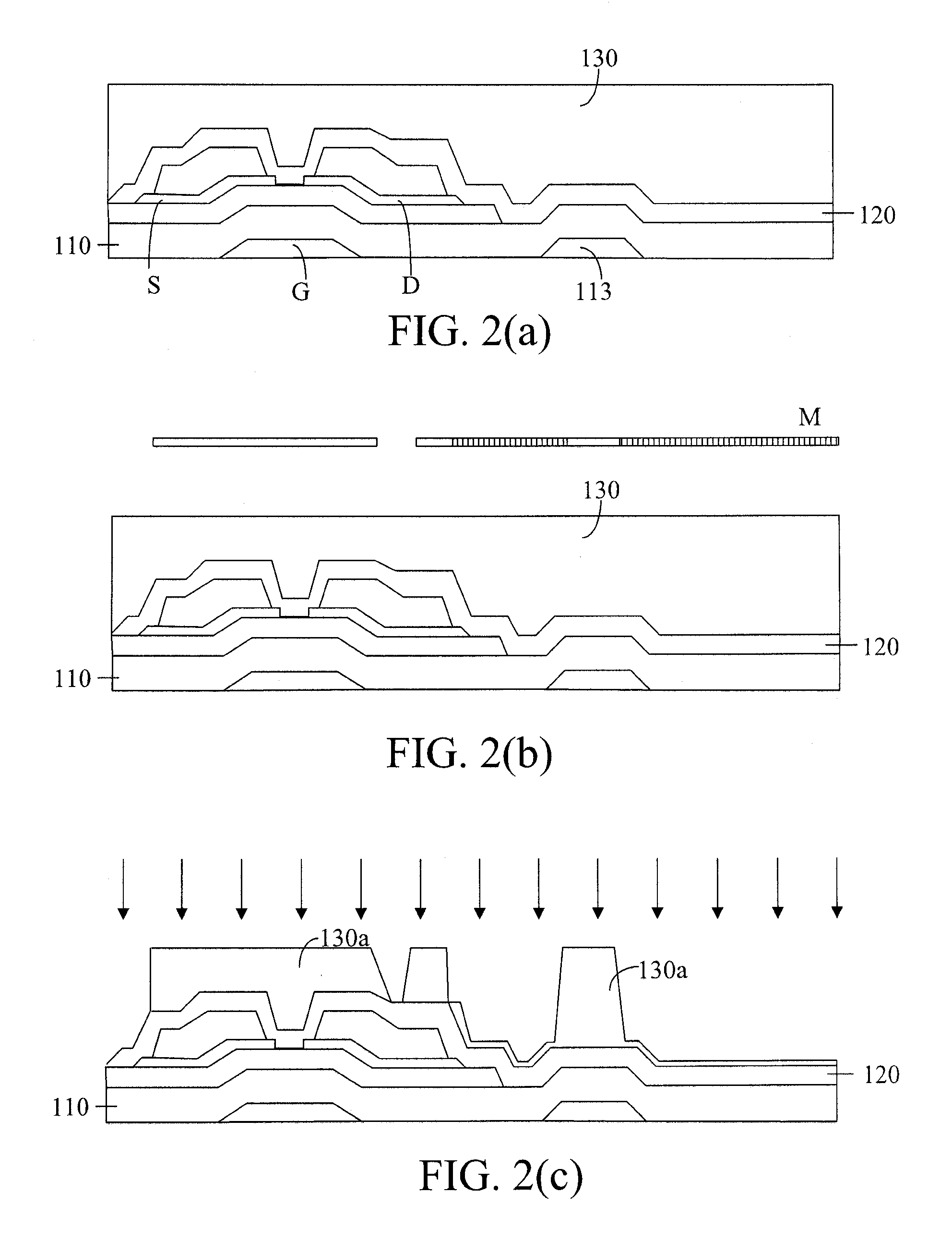
[0032]FIGS. 2(a) to 2(f) are cross sectional views schematically showing a manufacturing method for manufacturing the active array substrate 10 according to the first embodiment of the present invention.

[0033]As shown in FIG. 2(a), the base 110 is first provided, followed by forming the scan line 111, capacitor electrode 113, data line 112, active device (ex. thin film transistor TFT) and passivation 120 on the base 110. The thin film transistor TFT comprises a gate G, a source S and a drain D. Then, a photoresist layer 130 is formed, which completely covers the passivation 120. The photoresist layer 130 has an average thickness of about 0.5 micrometers to 5 micrometers.

[0034]Next, as shown in FIG. 2(b), provide a mask M above the photoresist layer 130. Mask M may be a half-tone mask or a grey-tone mask for example. The effect of the half-tone mask or grey-tone mask is understood by those skilled in the art and will not be discussed in detail herein. The photoresist layer is exposed...

second embodiment

[0039]FIGS. 3(a) to 3(g) are cross sectional views schematically showing a manufacturing method for manufacturing the active array substrate 10 according to the second embodiment of the present invention. Because FIGS. 3(a) to 3(g) are corresponding to the same manufacturing process as that of FIGS. 2(a) to 2(e), the reference number of the elements will continue to be used and the details will not be further described herein.

[0040]In FIG. 3(f), after curing the fluid color material 160 to form the color filter layers 140 and removing at least one portion of the patterned bank 130b, the fluid color material 160 is provided, which may be red, red or blue, on the thin film transistor TFT by ink jet printing IJP′ for the height auxiliary structure 141 which will be formed in later steps. Then, the fluid color material 160 is cured on the thin film transistor TFT to form the height auxiliary structure 141. Because the height auxiliary structure 141 is formed by the ink jet printing IJP′...

third embodiment

[0045]FIGS. 4(a) to 4(f) are cross sectional views schematically showing a manufacturing method for manufacturing the active array substrate 10 according to the third embodiment of the present invention.

[0046]FIGS. 4(a)-4(b) and description thereof are the same as that of FIGS. 2(a)-2(b), so detailed descriptions are omitted for convenience herein.

[0047]As shown in FIG. 4(c) the pattern of the patterned bank 130a is unlike FIG. 2(c). In the present embodiment, the capacitor region C is pre-defined.

[0048]Next, as shown in FIG. 4(e), the fluid color material 160 is provided by the ink jet printing IJP in the pixel region P defined within the patterned bank 130b. The fluid color material 160 is, for example, a dye, pigment or a combination thereof. The color of the fluid color material 160 is, for example, red, green or blue. Next, the fluid color material 160 is cured to form a plurality of the color filter layers 140.

[0049]Finally, as shown in FIG. 4(f), a pixel electrode 150 is form...


PUM


Abstract

An active array substrate, liquid crystal display panel, and manufacturing method thereof are provided. The active array substrate includes a base, a plurality of scan lines disposed on the base, a plurality of data lines perpendicular to the scan lines, a plurality of pixel electrodes, a plurality of active devices, in which each active device is connected to the corresponding scan line, data line and pixel electrode to form a pixel region. The height adjust structure, disposed on the active device, the data line or the scan line, can be shaped into a circle, circle-like shape, ellipse, a compact pattern without any acute angle or a compact pattern without any right angle.

Description

[0001]This application claims priority to Taiwan Patent Application No. 097104179, filed on Feb. 4, 2008, the disclosure of which is incorporated herein by reference in its entirety.CROSS-REFERENCES TO RELATED APPLICATIONS[0002]Not applicable.BACKGROUND OF THE INVENTION[0003]1. Field of the Invention[0004]The present invention generally relates to an active array substrate, a liquid crystal display panel and method for manufacturing the same; and particularly relates to an active array substrate having a color filter and method for manufacturing the same.[0005]2. Descriptions of the Related Art[0006]Conventional methods for manufacturing color filters use three color resists and three photolithography processes. The three color resists are sequentially formed in the pixel regions of a substrate to form a color filter. Because the color resists layers are formed by dropping the color resist liquid on the substrate and then performing spin coating, most color resists are wasted when c...

Claims


Application Information

Patent Timeline
IPC IPC(8): G02F1/1335
CPCG02F1/1362G02F1/13394
Inventor HUANG, YEN-HENGCHEN, CHUNG-KAILEE, SHU-CHIN
Owner AU OPTRONICS CORP
Why Eureka
Try Eureka