Method of driving electro-optical device and electronic apparatus

a technology of electrooptical devices and electronic devices, applied in the direction of static indicating devices, identification means, instruments, etc., can solve problems such as delay in displaying images, and achieve the effect of reducing the time for writing data and reducing the manufacturing cost of a display devi

Active Publication Date: 2009-08-20
ELEMENT CAPITAL COMMERCIAL CO PTE LTD
View PDF12 Cites 2 Cited by
  • Summary
  • Abstract
  • Description
  • Claims
  • Application Information

AI Technical Summary

Benefits of technology

[0007]The smaller data signals are, the longer a period of time for writing the data signals in the storage capacitors (hereinafter, referred to as writing time) is. In particular, when it is desired to emit light from the organic EL elements at low brightness, the time for writing the data signals in the storage capacitors is longer due to the wiring capacitance of the data lines and the like, thereby causing delay in displaying images. Accordingly, an object of the present invention is to provide a method of driving an electro-optical device and an electronic apparatus, which are capable of reducing the time for writing data without providing special circuits.

Problems solved by technology

In particular, when it is desired to emit light from the organic EL elements at low brightness, the time for writing the data signals in the storage capacitors is longer due to the wiring capacitance of the data lines and the like, thereby causing delay in displaying images.

Method used


Image

  • Method of driving electro-optical device and electronic apparatus
  • Method of driving electro-optical device and electronic apparatus
  • Method of driving electro-optical device and electronic apparatus

Examples


first embodiment

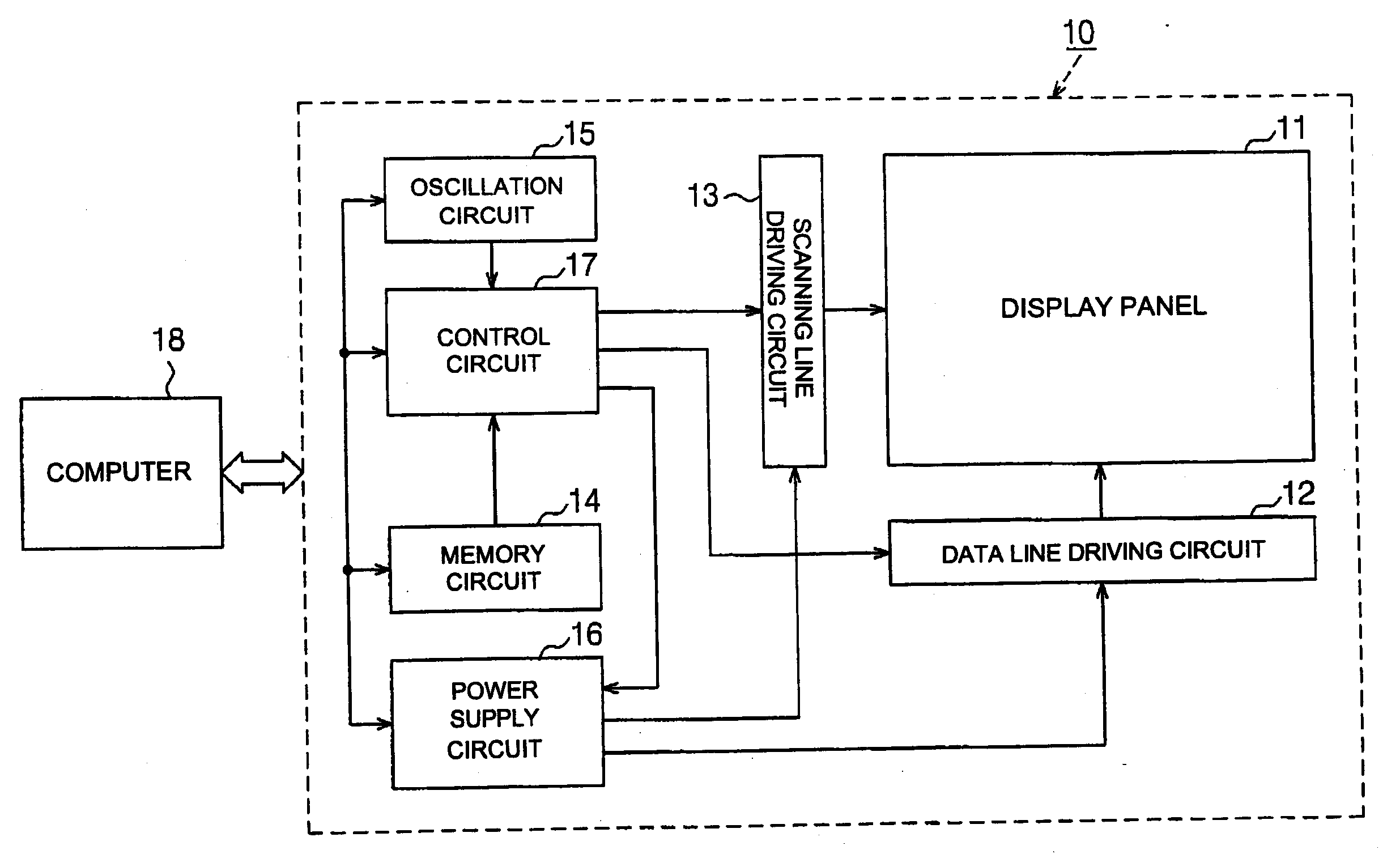
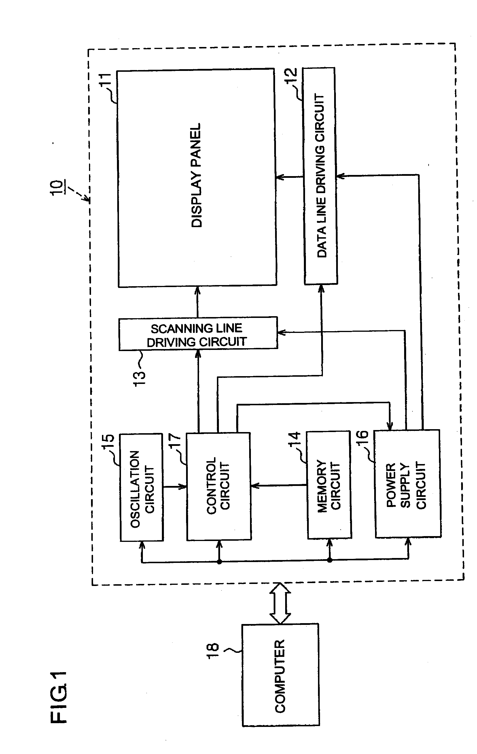
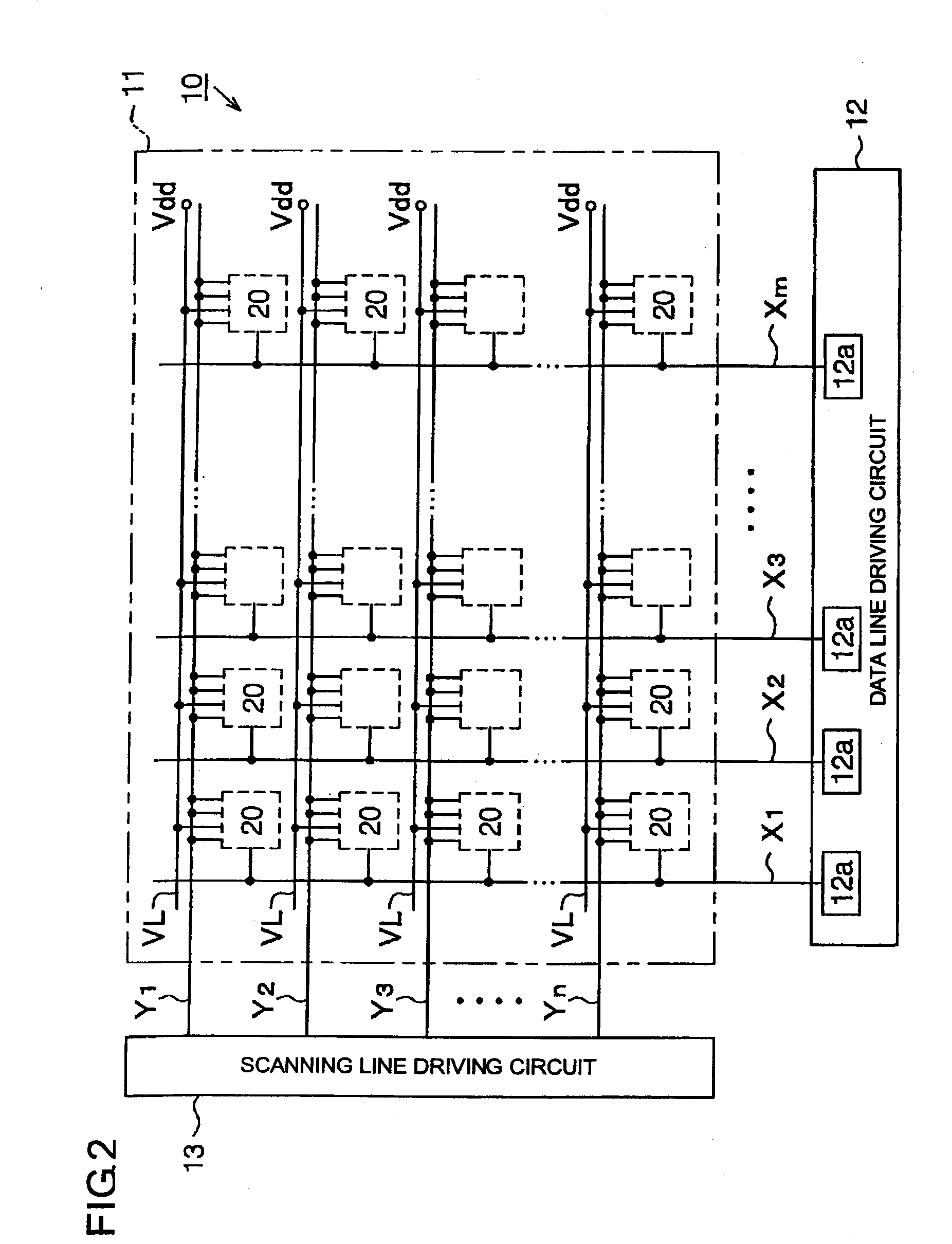
[0038]the present invention will be described with reference to FIGS. 1 to 4. FIG. 1 is an exemplary block circuit diagram illustrating the electrical structure of an organic EL display 10. FIG. 2 is an exemplary block circuit diagram illustrating the electrical structure of a display panel, a data line driving circuit, and a scanning line driving circuit.

[0039]In FIG. 1, the organic EL display 10 can include a display panel 11, a data line driving circuit 12, a scanning line driving circuit 13, a memory circuit 14, an oscillation circuit 15, a power supply circuit 16, and a control circuit 17. The respective elements 11 to 17 of the organic EL display 10 may be formed of independent electronic parts. For example, each of the elements 11 to 17 may be formed of a one-chip semiconductor integrated circuit device. Further, all or some of the elements 11 to 17 may be formed of an integrated electronic part. For example, the data line driving circuit 12 and the scanning line driving circ...

second embodiment

[0082] the drain of the driving transistor Qd is connected to the anode of the organic EL element 21. The cathode of the organic EL element 21 is grounded. The source of the driving transistor Qd is connected to the power line VL. The gate of the driving transistor Qd is electrically connected to the coupling capacitor Cp, the storage capacitor Co, and the controlling transistor Qct.

[0083]Specifically, the gate of the driving transistor Qd is connected to the first electrode La of the coupling capacitor Cp. The second electrode Lb of the coupling capacitor Cp is connected to the drain of the switching transistor Qsw. The gate of the switching transistor Qsw is connected to the first sub-scanning line Y11 that constitutes the first scanning line Y1.

[0084]The gate of the driving transistor Qd is connected to the third electrode Lc of the storage capacitor Co. The fourth electrode Ld of the storage capacitor Co is connected to the power line VL. The gate of the driving transistor Qd is...


PUM


Abstract

The invention provides a method of driving an electro-optical device and an electronic apparatus which are capable of reducing the time for writing data without providing special circuits. In the electro-optical device pixel circuits having reset transistors for controlling an electric connection between drains and gates of driving transistors between the drains and the gates of the driving transistors are arranged on a display panel in a matrix. The pixel circuits arranged in a matrix are electrically connected to a scanning line driving circuit via scanning lines. The scanning line driving circuit sequentially switches on the reset transistors from the pixel circuit connected to first scanning lines in accordance with scanning line control signals supplied from a control circuit and then lets organic EL elements emit light.

Description

[0001]This is a continuation of application Ser. No. 10 / 773,410 filed Feb. 9, 2004, which claims the benefit of Japanese Patent Publication No. 2003-033666 filed Feb. 12, 2003. The disclosures of the prior applications are hereby incorporated by reference herein in their entirety.BACKGROUND OF THE INVENTION[0002]1. Field of Invention[0003]The present invention relates to a method of driving an electro-optical device and an electronic apparatus.[0004]2. Description of Related Art[0005]One method of driving a display device using organic EL elements as electro-optical elements can include an active matrix driving method in which a plurality of pixel circuits for controlling the brightness of respective organic electroluminescent (EL) elements are arranged in a matrix. Each of the pixel circuits includes a transistor for controlling the driving current supplied to the organic EL element and a storage capacitor for storing voltage corresponding to a data voltage for controlling the elec...

Claims


Application Information

Patent Timeline
Patent Type & Authority Applications(United States)
IPC IPC(8): G09G5/00H01L51/50G09F9/30G09G3/20G09G3/30G09G3/32H05B33/02H05B33/14
CPCG09G3/3233G09G2300/0819G09G2300/0852G09G2300/0861G09G2320/043G09G2310/0251G09G2310/0262G09G2320/0223G09G2310/0224A61F13/565A61F13/58A61F13/62A61F2013/4909
Inventor MIYAZAWA, TAKASHI
Owner ELEMENT CAPITAL COMMERCIAL CO PTE LTD
Why Eureka
Try Eureka