Apperance inspection apparatus with scanning electron microscope and image data processing method using scanning electron microscope

a scanning electron microscope and image data processing technology, applied in the field of appearance inspection apparatuses, can solve the problems of reducing the intensity of a luminance signal, affecting the manufacturing yield of semiconductor devices, and inadequate contrast, and achieve the effect of improving throughpu

Inactive Publication Date: 2009-08-20
HITACHI HIGH-TECH CORP
View PDF15 Cites 8 Cited by
  • Summary
  • Abstract
  • Description
  • Claims
  • Application Information

AI Technical Summary

Benefits of technology

[0017]The present invention allows a user to give precedence to S / N improvement over throughput improvement, or vice versa.

Problems solved by technology

In semiconductor device manufacture, the results of lithographic, etching, or other processes, and defects caused by, for example, foreign matter significantly affect the manufacturing yield of semiconductor devices.
In an inspection apparatus using such a scanning electron microscope (SEM), the quantity of electron beam emitted onto a sample is insufficient, resulting in inadequate contrast.
However, if the period of the final digital image signal is shortened, scanning speed must also be increased, which would decrease the intensity of a luminance signal, and hence the S / N ratio.
Any decrease in the S / N ratio degrades accuracy in defect detection.
However, the time for which an image is captured is lengthened and, accordingly, the throughput degrades.
However, conventional technology does not allow a user to give precedence to defect detection performance over throughput or vice versa as a user's desire.

Method used


Image

  • Apperance inspection apparatus with scanning electron microscope and image data processing method using scanning electron microscope
  • Apperance inspection apparatus with scanning electron microscope and image data processing method using scanning electron microscope
  • Apperance inspection apparatus with scanning electron microscope and image data processing method using scanning electron microscope

Examples


Embodiment Construction

[0026]The present invention is applicable in any device that captures an image by use of a scanning electron microscope. However, the description below is given using an example where the present invention is applied in an SEM type appearance inspection apparatus.

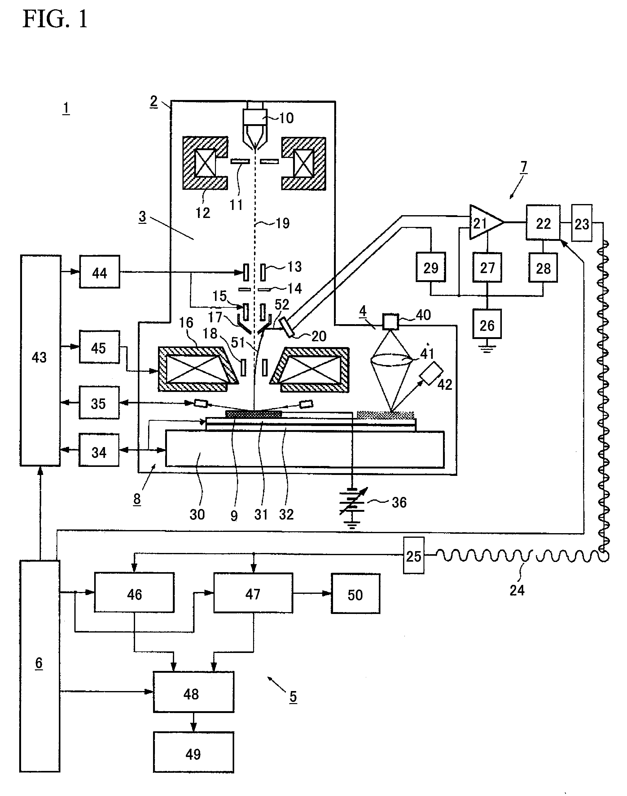
[0027]An example of the configuration of an SEM type appearance inspection apparatus according to this example will be described with reference to FIG. 1. The SEM type appearance inspection apparatus 1 includes an inspection chamber 2. The inspection chamber 2 has an electron optical system device 3, optical microscope 4, and sample chamber 8.

[0028]The electron optical system device 3 has an electron gun 10, an extraction electrode 11 for electron beams, a condenser lens 12, a blanking deflector 13, an aperture 14, a scanning deflector 15, an objective lens 16, a conical beam reflector 17, an E×B deflector 18, and a secondary electron detector 20. The blanking deflector 13 deflects an electron beam 19 to the outside of the ...


PUM


Abstract

The present invention provides an appearance inspection apparatus that allows a user to give precedence to either defect detection performance or throughput. The appearance inspection apparatus allows a user to select the frequency of a digital image signal or the ratio of the frequency of the digital image signal to a sampling rate. Further, a user is allowed to select either throughput improvement or S/N improvement to prioritize.

Description

BACKGROUND OF THE INVENTION[0001]1. Field of the Invention[0002]The present invention relates to appearance inspection apparatuses for inspecting defects in samples and more particularly relates to technology for inspecting the appearance of samples by use of scanning electron microscopes (SEM).[0003]2. Description of the Related Art[0004]Memories used in computers and the like, and semiconductor devices such as microcomputers are produced in the following manner: a pattern such as a circuit formed on a photo mask is repeatedly transferred by an exposure process, lithographic process, etching process, or the like. In semiconductor device manufacture, the results of lithographic, etching, or other processes, and defects caused by, for example, foreign matter significantly affect the manufacturing yield of semiconductor devices. Therefore, it is necessary to detect abnormalities or faults at an early stage or in advance. In order to detect these, patterns on semiconductor wafers are i...

Claims


Application Information

Patent Timeline
Patent Type & Authority Applications(United States)
IPC IPC(8): G06K9/00
CPCH01J37/222H01J37/244H01J37/28H01J2237/2817H01J2237/24495H01J2237/2485H01J2237/221
Inventor OMINAMI, YUSUKEMIYAI, HIROSHIGUNJI, YASUHIRO
Owner HITACHI HIGH-TECH CORP
Why Eureka
Try Eureka