Bus interconnect device and a data processing apparatus including such a bus interconnect device

a bus interconnect and data processing technology, applied in coupling devices, electrical apparatus construction details, waveguides, etc., can solve the problems of increasing complexity of apparatuses, increasing multi-path effects, and increasing the complexity of components of data processing apparatuses, so as to reduce multi-path effects, reduce interconnect speed and latency, and simplify transmitter circuitry

Active Publication Date: 2009-08-20
ARM LTD
View PDF38 Cites 3 Cited by
  • Summary
  • Abstract
  • Description
  • Claims
  • Application Information

AI Technical Summary

Benefits of technology

[0018]In accordance with the present invention, the use of parallel plates removes the requirement to specifically route a conductor between the various devices that are to use the waveguide. Instead the devices merely need to be coupled into the waveguide at an arbitrary location within one of the parallel plates, and thereafter can transmit signals to, and receive signals from, any other device coupled into the waveguide. This approach hence alleviates the layout complexity associated with prior art MTL or CPW techniques.
[0041]Embodiments of the invention alleviate the issues of interconnect speed and latency by using RF or optical propagation to avoid the parasitic losses of conventional tracks. Certain embodiments also ease the layout task by providing a global communications resource that can be tapped into from any block in a multi-chip system.

Problems solved by technology

The design of components for a data processing apparatus is a labour intensive task, and becomes more complex as data processing apparatus increase in complexity.
As data processing apparatus increase in complexity, the number of master and slave devices to be interconnected increases, as do the number of ways in which those master and slave devices can be connected.
This significantly increases the complexity of the design of the bus interconnect, and in particular the various connections specified by the bus interconnect.
In particular, in addition to propagation delay within the interconnect, parasitic losses contribute significantly to the latency of the interconnect.
To seek to alleviate delay within the interconnect, buffers can be added in the communication paths of the interconnect to improve speed of propagation of signals, but such buffers increase power consumption.
Further, such delays complicate attainment of data coherency at selected points in the system.
Conventional interconnect techniques require a significant amount of extra effort at the physical layout stage to adequately buffer the data paths and to remove skew between clock and data.
As a result routing is complex and expensive due to the number of layers required.
When designing data processing apparatus, particularly with system-on-chip (S-o-C), it is becoming increasingly difficult to achieve the desired clock rates with current interconnect techniques.
Whilst such approaches can reduce the wiring requirement of the interconnect (due to the serial communication), such interconnects are difficult to design and are based on point-to-point communication.
Further, none of the above prior art approaches address the underlying process problems of high resistance and capacitance.
It is especially difficult to achieve high data rates when the interconnect is “off-chip”, that is where the interconnect passes data between the chip and another device.
However, this comes at the cost of much more stringent design rules and restricted interconnect topologies.
As such, whilst such techniques can alleviate the earlier mentioned resistance and capacitance problems exhibited in traditional interconnect systems based on electrical conduction through wired connections, they still give rise to routing issues due to the need to specifically route the conductor of the waveguide between the various components that are to communicate via that waveguide.
Hence, the design of such interconnects is still relatively complex.

Method used


Image

  • Bus interconnect device and a data processing apparatus including such a bus interconnect device
  • Bus interconnect device and a data processing apparatus including such a bus interconnect device
  • Bus interconnect device and a data processing apparatus including such a bus interconnect device

Examples


Embodiment Construction

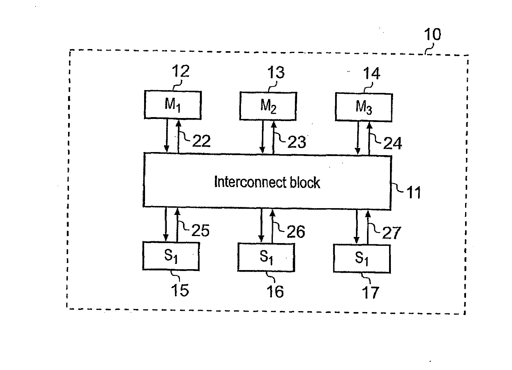
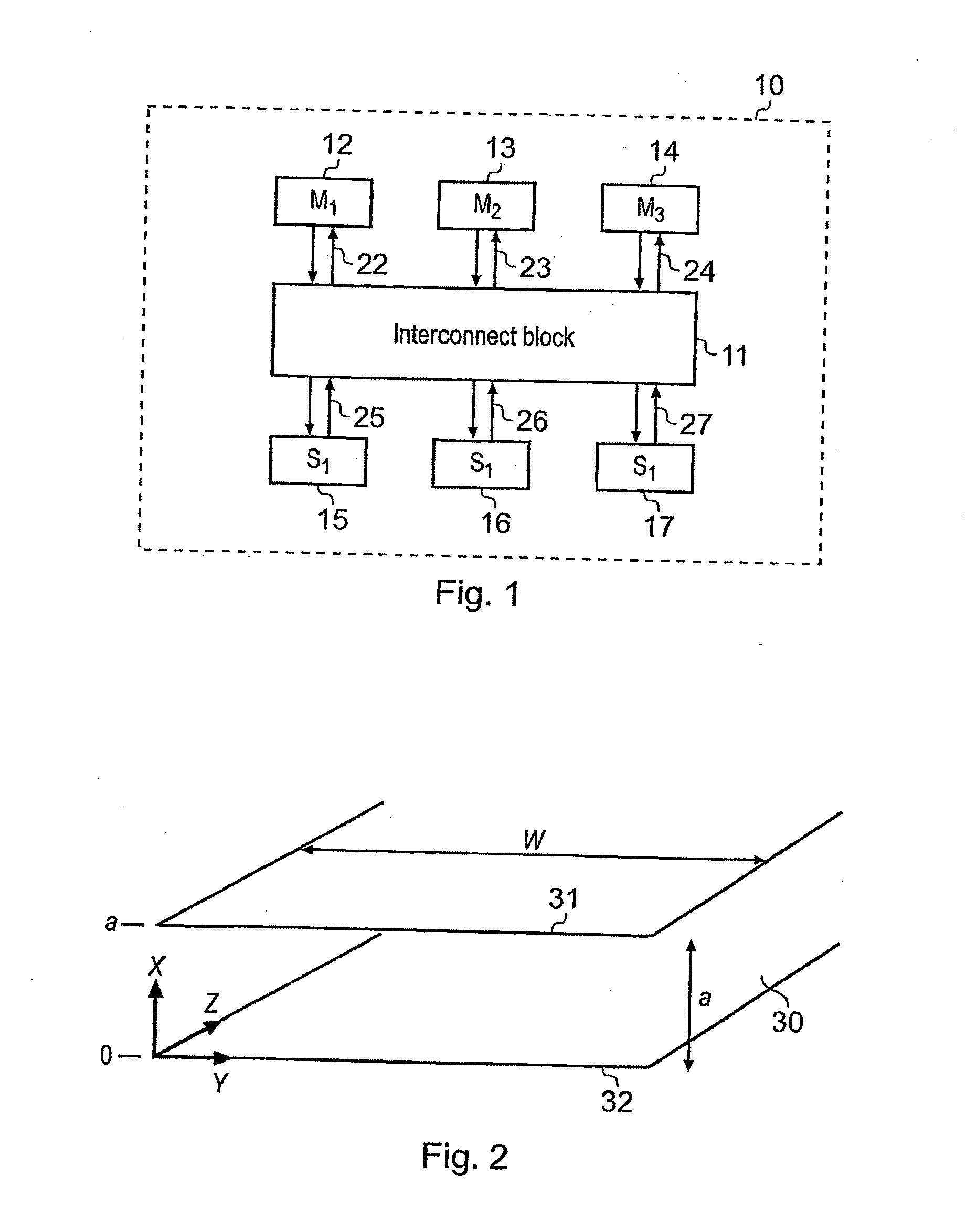
[0050]For example, FIG. 1 illustrates a data processing apparatus in the form of a System-on-Chip (S-o-C), which may be used within a device such as a personal organiser, a mobile phone, a television set-top box, etc. The S-o-C 10 has a plurality of devices or functional blocks (also known as IP blocks) 12, 13, 14, 15, 16, 17 that are interconnected by an arrangement of buses. The actual interconnection of these buses is specified within an interconnect block 11. The interconnect block 11 includes a matrix of connections which provides for the interconnection of multiple bus master devices and bus slave devices within the S-o-C 10.

[0051]Hence, each master device 12, 13, 14 may be connected to corresponding buses 22, 23, 24 respectively, whilst each slave device 15, 16, 17 may also be connected to corresponding buses 25, 26, 27 respectively, with the interconnect block 11 defining how these various buses are interconnected.

[0052]The buses interconnecting the various elements will typ...


PUM


Abstract

A bus interconnect device is provided comprising a parallel plate waveguide for coupling together a plurality of devices. This provides an efficient and flexible approach for providing interconnect functionality within a data processing apparatus.

Description

FIELD OF THE INVENTION[0001]The present invention relates to a bus interconnect device and to a data processing apparatus including such a bus interconnect device, and in particular to a technique for improving bus interconnect devices.BACKGROUND OF THE INVENTION[0002]The design of components for a data processing apparatus is a labour intensive task, and becomes more complex as data processing apparatus increase in complexity. One such component is a bus interconnect which is used to define the bus connections between various other components within the data processing apparatus. In particular, the bus interconnect will define the bus infrastructure that allows a number of master devices to access a number of slave devices. As data processing apparatus increase in complexity, the number of master and slave devices to be interconnected increases, as do the number of ways in which those master and slave devices can be connected. This significantly increases the complexity of the desi...

Claims


Application Information

Patent Timeline
Patent Type & Authority Applications(United States)
IPC IPC(8): G06F13/42G06F13/14
CPCH01P3/02
Inventor BRUCE, ALISTAIR CRONETUNE, ANDREW DAVID
Owner ARM LTD
Why Eureka
Try Eureka