Flexible Printed Circuit Assembly With Reduced Dielectric Loss

a printed circuit and dielectric loss technology, applied in the direction of printed circuit aspects, printed circuit manufacturing, high-frequency circuit adaptations, etc., can solve the problems of poor i/o density, high-performance coax or optical fiber, and traditional wire cables cannot meet the requirements of high-speed signal interconnection, etc., to reduce the overall thickness of the assembly, reduce the dielectric loss, and reduce the tangent of the dielectric loss

Inactive Publication Date: 2009-08-27
IBM CORP +1
View PDF2 Cites 16 Cited by
  • Summary
  • Abstract
  • Description
  • Claims
  • Application Information

AI Technical Summary

Benefits of technology

[0013]In a further exemplary aspect of the invention, the second dielectric layer may be made of fluorocarbon or other material that has a dielectric loss tangent much smaller than that of any bonding material forming the adhesive layer.

Problems solved by technology

As processing speeds and packaging densities have increased, traditional wire cables cannot meet the requirements of high-speed signal interconnections.
Further, high-performance coax or optical fiber has drawbacks, such as, poor I/O density, a greater overall cost, lack of decoupling and DC distribution, and a greater consumption of precious physical space.
Because of the relatively large dielectric loss tange

Method used


Image

  • Flexible Printed Circuit Assembly With Reduced Dielectric Loss
  • Flexible Printed Circuit Assembly With Reduced Dielectric Loss

Examples


Embodiment Construction

[0016]The invention will now be described in more detail by way of example with reference to the embodiments shown in the accompanying figures. It should be kept in mind that the following described embodiments are only presented by way of example and should not be construed as limiting the inventive concept to any particular physical configuration.

[0017]Further, if used and unless otherwise stated, the terms “upper”, “lower”, “front”, “back”, “over”, “under”, and similar such terms are not to be construed as limiting the invention to a particular orientation. Instead, these terms are used only on a relative basis.

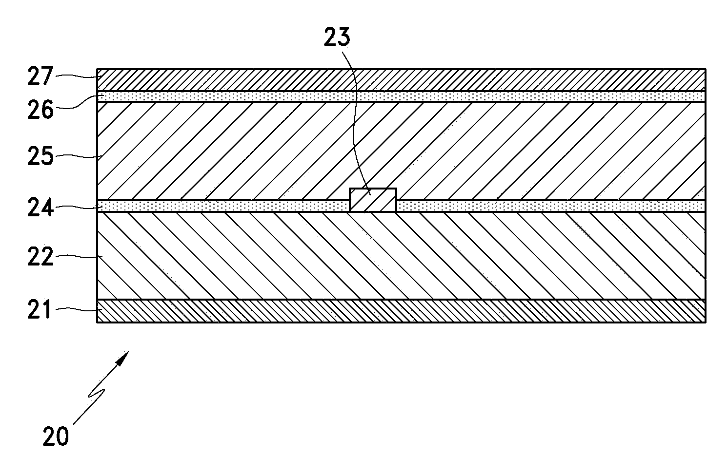
[0018]FIG. 2 is a schematic cross-sectional view of a flexible printed circuit assembly 20, according to an exemplary embodiment of the present invention. The flexible printed circuit assembly 20 may have a similar layer structure of the assembly 10, as shown in FIG. 1. Referring to FIG. 2, the flexible printed circuit assembly 20 includes a bottom ground layer 21, a first...


PUM

PropertyMeasurementUnit
Dielectric polarization enthalpyaaaaaaaaaa
Flexibilityaaaaaaaaaa
Electrical conductoraaaaaaaaaa

Abstract

A flexible printed circuit assembly with a fluorocarbon dielectric layer and an adhesive layer with reduced thickness. The flexible printed circuit assembly includes a first dielectric layer and a signal trace disposed on the first dielectric layer. An adhesive layer with a thickness smaller than a height of the signal trace is disposed on the first dielectric layer, so that only a portion of a side surface of the signal trace is covered. A second dielectric layer made of fluorocarbon is disposed on the adhesive layer, covering a remaining portion of the side surface of the signal trace and a top surface of the signal trace.

Description

BACKGROUND OF THE INVENTION[0001]1. Field of the Invention[0002]The invention relates to a flexible printed circuit assembly, and in particular, to a flexible multilayer printed circuit assembly that effectively reduces dielectric loss and decreases overall construct thickness by using a fluorocarbon dielectric layer, and an adhesive layer after lamination that is thinner than a signal trace.[0003]2. Background Information[0004]As processing speeds and packaging densities have increased, traditional wire cables cannot meet the requirements of high-speed signal interconnections. Further, high-performance coax or optical fiber has drawbacks, such as, poor I / O density, a greater overall cost, lack of decoupling and DC distribution, and a greater consumption of precious physical space. Thus, flexible printed circuit assemblies have been developed for the high-speed interconnections between multiple computer processing units. These flexible printed circuit assemblies are high circuit den...

Claims


Application Information

Patent Timeline
IPC IPC(8): H05K1/02H05K3/36
CPCH05K1/024H05K1/0393H05K3/386H05K3/4626H05K3/4635Y10T29/49128H05K2201/015H05K2201/0191H05K2201/0715Y10T29/49126Y10T29/49163H05K3/4688
Inventor ABRAHAMSON, PAUL V.DANGLER, JOHN RICHARDDAWIEDEZYK, DANIEL LEEDOYLE, MATTHEW STEPHEN
Owner IBM CORP
Why Eureka
Try Eureka