Liquid crystal display device and manufacturing method therefor
a display device and liquid crystal technology, applied in the field of display devices, can solve the problems of reducing the thickness of the substrate, the limitation of the bending degree the inability to make flexible display devices which can be freely bent using the glass substrate, so as to improve the flexibility of the display device, the display surface of the display device is curved, and the design selectivity of the display device is increased.
- Summary
- Abstract
- Description
- Claims
- Application Information
AI Technical Summary
Benefits of technology
Problems solved by technology
Method used
Image
Examples
embodiment 1
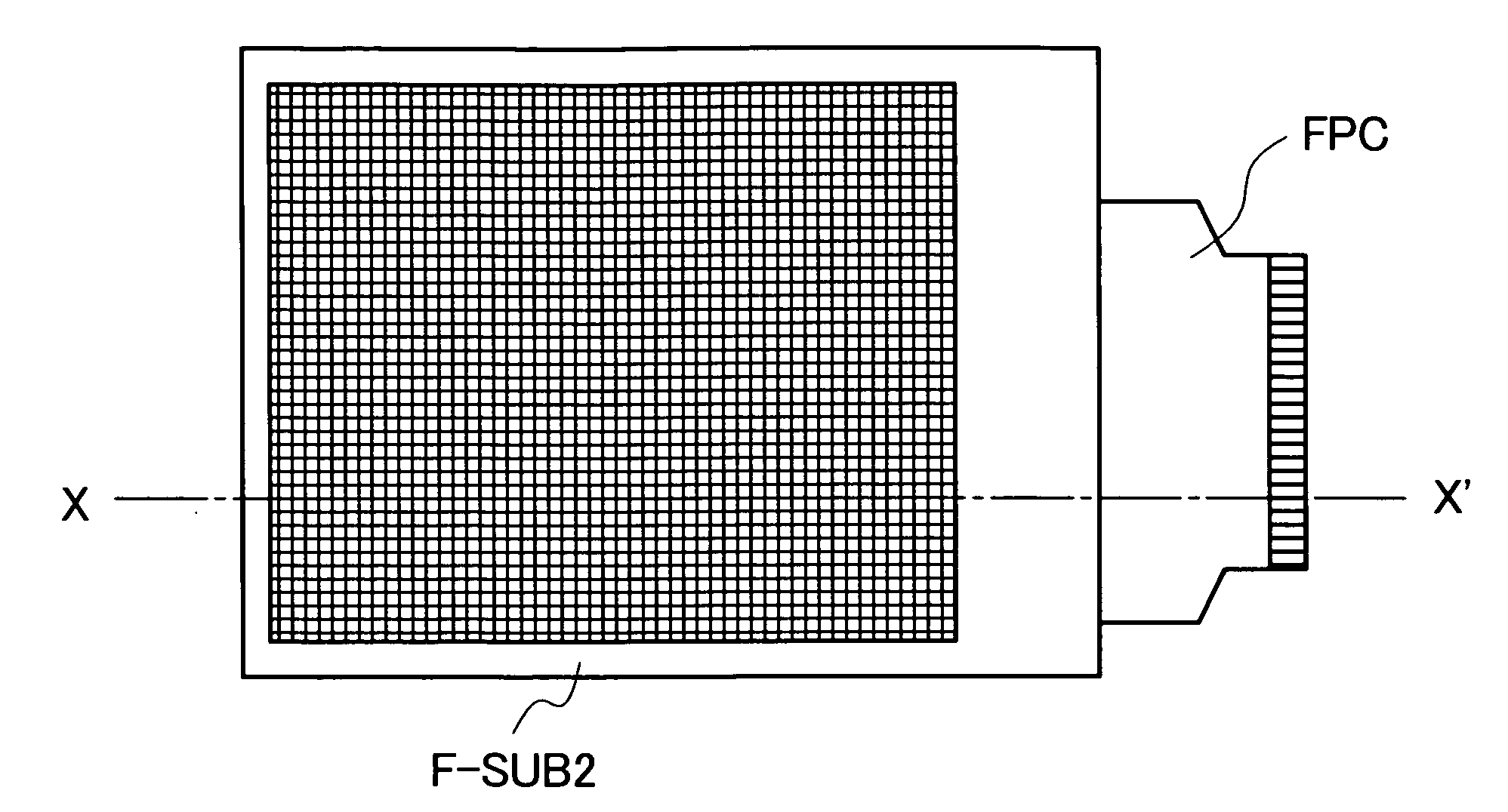
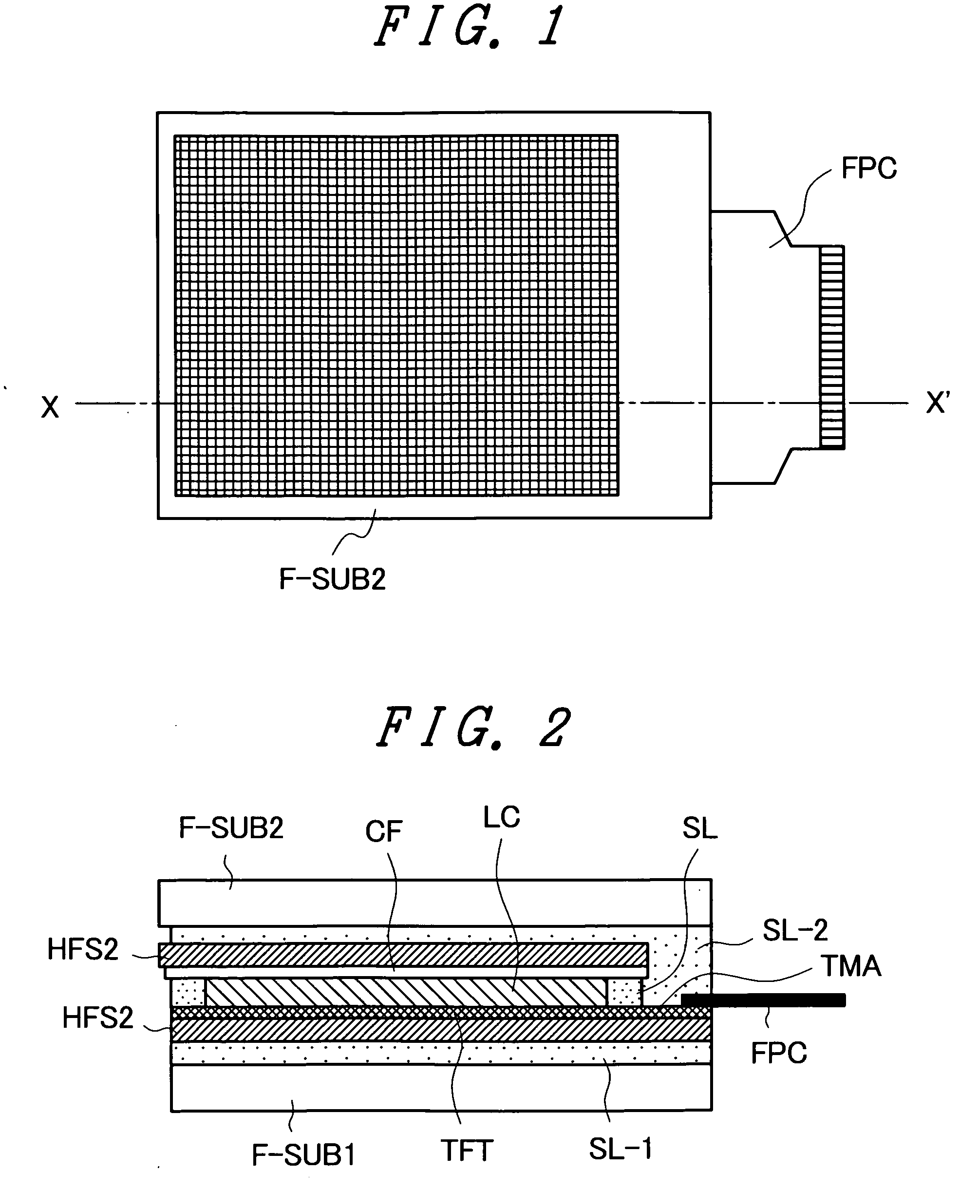
[0024]FIG. 1 is a plan view of a liquid crystal display device illustrating an embodiment 1 of a display device of the invention. FIG. 2 is a sectional view taken along line X-X′ of FIG. 1. The liquid crystal display device of the embodiment 1 shown in FIG. 1 is configured by sealing in a liquid crystal LC between a principal surface of a TFT side flexible substrate F-SUB1, which is a first plastic substrate, and a principal surface of a CF side flexible substrate F-SUB2, which is a second plastic substrate, and bonding them together with a frame shaped seal agent SL encircling a display area.
[0025]A feature of the embodiment lies in adopting a structure in which a wiring substrate FPC is sandwiched between the TFT side flexible substrate F-SUB1 and the CF side flexible substrate F-SUB 2.
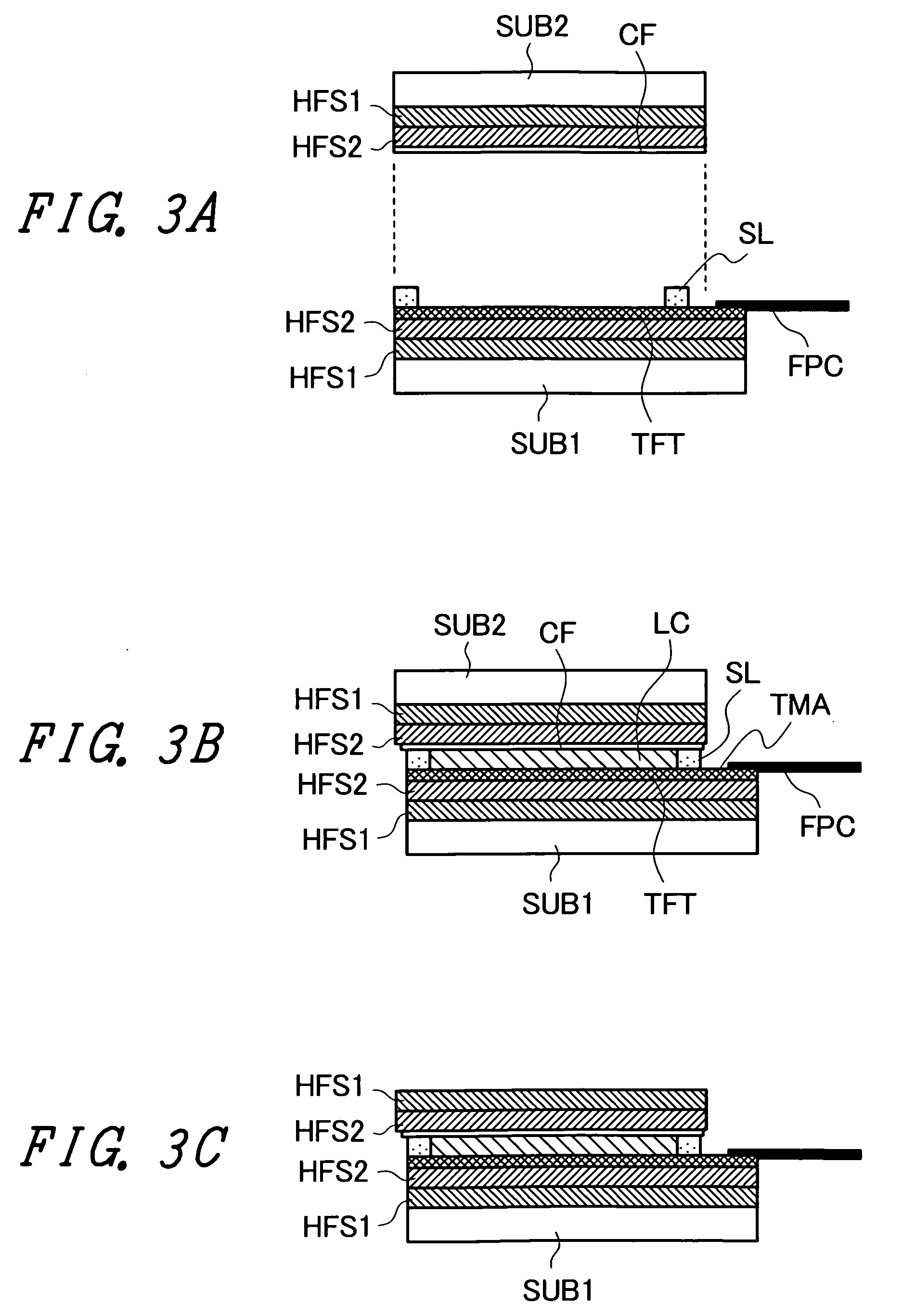
[0026]As shown in FIG. 2, on the principal surface of the TFT side flexible substrate F-SUB1 is formed a silicon nitride layer (a second etch stopper layer HFS2 to be described hereafter) which, bei...
embodiment 2
[0041]Next, a description will be given of an embodiment 2 of the invention.
[0042]FIG. 4 is a sectional view of a liquid crystal display device illustrating the embodiment 2 of the display device of the invention. FIG. 4 corresponds to the section taken along line X-X′ of FIG. 1. The liquid crystal display device of the embodiment 2 shown in FIG. 4 is configured by sealing in a liquid crystal LC between a principal surface of a thin film transistor substrate SUB1, which is a glass substrate, and a principal surface of a CF side flexible substrate F-SUB2, which is a plastic substrate, and bonding them together with a frame shaped seal agent SL encircling a display area.
[0043]A feature of the embodiment lies in adopting a structure in which a wiring substrate FPC is sandwiched between the thin film transistor substrate SUB1, which is the glass substrate, and the CF side flexible substrate F-SUB 2.
[0044]As shown in FIG. 4, the principal surface of the CF side flexible substrate F-SUB2 ...
PUM
| Property | Measurement | Unit |
|---|---|---|
| flexible | aaaaa | aaaaa |
| temperature | aaaaa | aaaaa |
| heat resistance | aaaaa | aaaaa |
Abstract
Description
Claims
Application Information


