Multiple derating factor sets for delay calculation and library generation in multi-corner STA sign-off flow

a technology of derating factor and delay calculation, applied in the field of computer delay, can solve the problems of inability to handle the layout of the entire circuit, inability to logical and physical design without the aid of computers, and too time-consuming to build every cell in silicon, etc., and achieve the effect of increasing accuracy

Inactive Publication Date: 2009-08-27
BELL SEMICON LLC
View PDF6 Cites 12 Cited by
  • Summary
  • Abstract
  • Description
  • Claims
  • Application Information

AI Technical Summary

Benefits of technology

[0030]Accordingly, an aspect of the present invention is a method to increase the accurac...

Problems solved by technology

Typically it is too time-consuming to build every cell in silicon and measure actual cell delays, instead, designers simulate the delay in a cell, a process called characterization.
Due to the large number of components and the exacting details required by the fabrication process, logical and physical design is not practical without the aid of computers.
Layout of the en...

Method used


Image

  • Multiple derating factor sets for delay calculation and library generation in multi-corner STA sign-off flow
  • Multiple derating factor sets for delay calculation and library generation in multi-corner STA sign-off flow
  • Multiple derating factor sets for delay calculation and library generation in multi-corner STA sign-off flow

Examples


Embodiment Construction

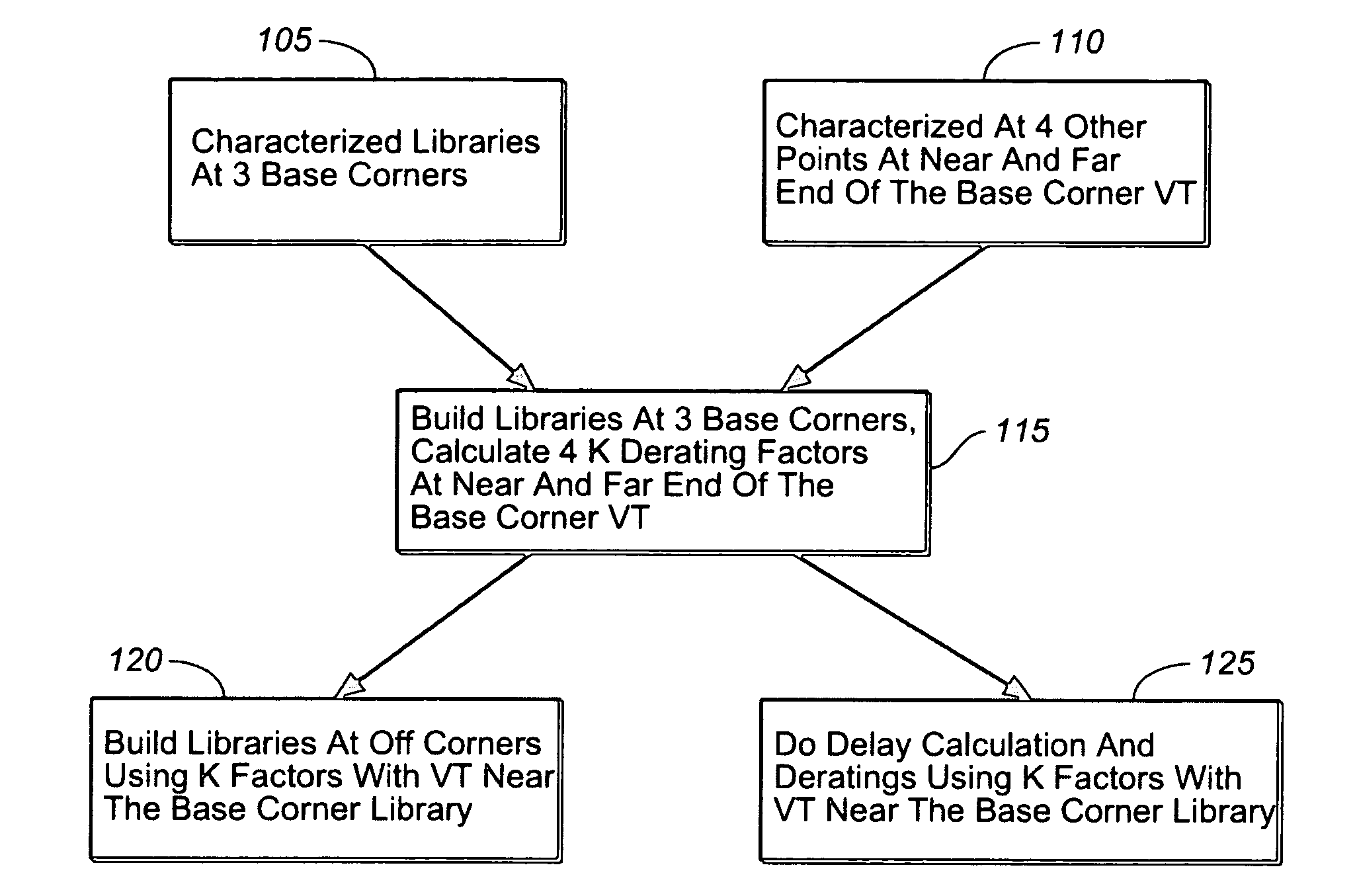
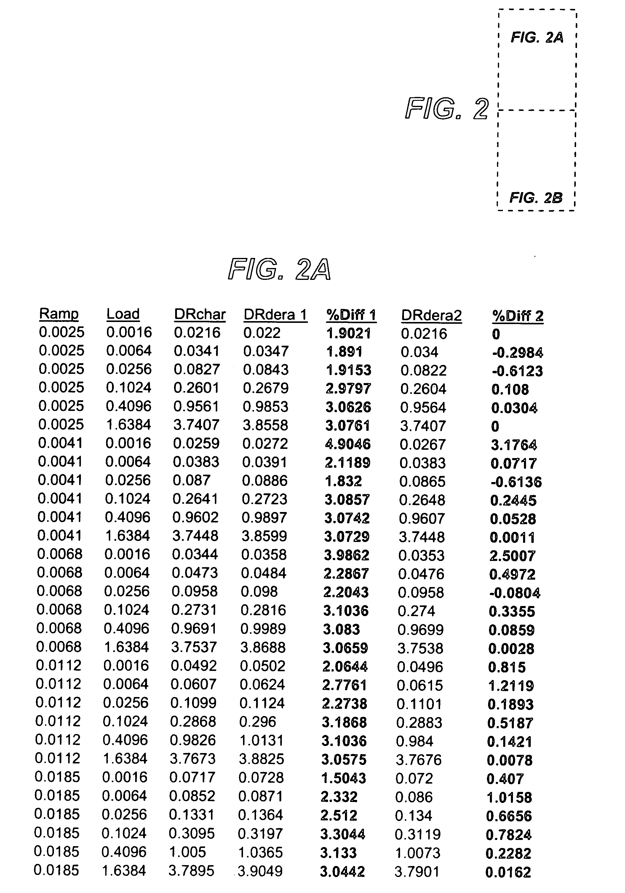
[0042]The present invention is a method to insert multiple corner deratings for delay calculations and library generation in a multi-corner STA sign-off methodology. An apparatus and method is disclosed to characterize a new process using an improved delay calculation. Multiple derating factors are used for different STA sign off corners. The approach of the present invention does not add any extra work in cell library characterization, while in the mean it increases the accuracy of the delay calculation and the library generation at corners other than standard corners.

[0043]In a preferred embodiment, the method and apparatus of the present invention can employ a mainframe or personal computer to run any software tool that incorporates the invention, and in general any compatible piece of hardware or virtual machine can run the present invention, in particular during the logical and physical design of a circuit such as an ASIC. Thus a preferred method and apparatus of the present in...


PUM


Abstract

An apparatus and method to characterize a new process using an improved delay calculation. Multiple derating factors are used for different STA sign off corners that have a base corner with two pairs of off-corners. The approach of the present invention does not add any extra work in cell library characterization, while in the mean it increases the accuracy of the delay calculation and the library generation at corners other than standard corners.

Description

CROSS-REFERENCE TO RELATED APPLICATIONS[0001][none]BACKGROUND OF THE INVENTION[0002]1. Field of Invention[0003]The present invention relates generally to the art of microelectronic integrated circuits. In particular, the present invention relates to the art of computing delays for cells in ASICs.[0004]2. Description of Related Art[0005]An integrated circuit chip (hereafter referred to as an “integrated circuit” (IC), “ASIC”, or a “chip”) comprises cells and connections between the cells formed on a surface of a semiconductor substrate. The IC may include a large number of cells and require complex connections between the cells.[0006]A cell is a group of one or more circuit elements such as transistors, capacitors, and other basic circuit elements grouped to perform a function. Each of the cells of an IC may have one or more pins, each of which, in turn, may be connected to one or more other pins of the IC by wires. The wires connecting the pins of the IC are also formed on the surfa...

Claims


Application Information

Patent Timeline
IPC IPC(8): G06F17/50
CPCG06F2217/84G06F17/5031G06F30/3312G06F2119/12
Inventor CUI, QIANBHUTANI, SANDEEP
Owner BELL SEMICON LLC
Why Eureka
Try Eureka