Organic Photoactive Device
- Summary
- Abstract
- Description
- Claims
- Application Information
AI Technical Summary
Benefits of technology
Problems solved by technology
Method used
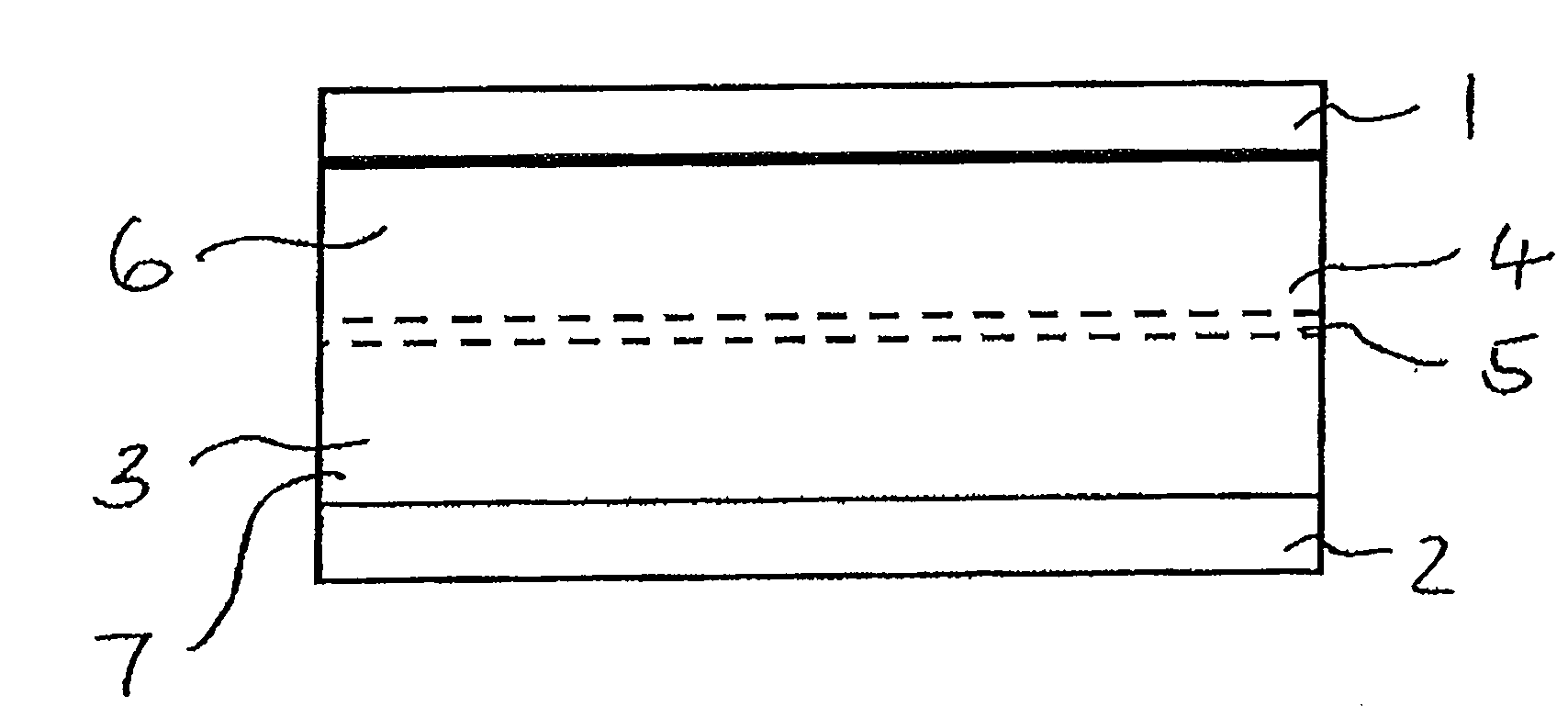
Image

Examples
example 1
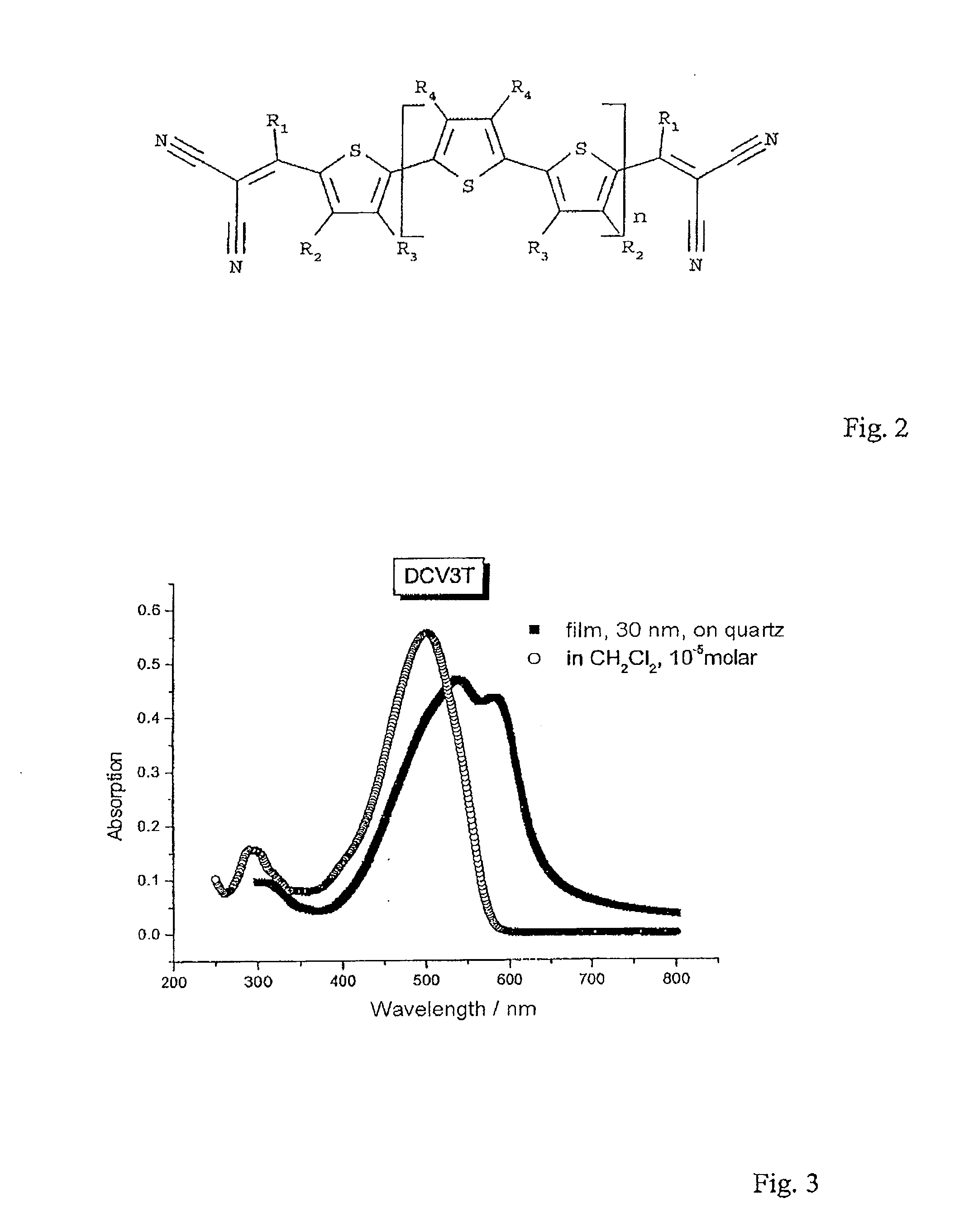
[0120]In a first example DCV3T (cf. structure in FIG. 5 with n=1 and group R1=hydrogen atom) is used as acceptor molecule in a heterojunction with N,N,N′,N′-tetrakis(4-methoxyphenyl) benzidine (MeOTPD) as donor molecule. A possible layer sequence for such a heterojunction, inserted into an M-i-p structure, is: Glass substrate / ITO / C60 (optional as electron transport layer) / DCV3T / MeOTPD / p-doped MeOTPD / p-doped zinc phthalocyanine (ZnPc; optional for improving the ohmic contact) / gold.
[0121]Since MeOTPD is largely transparent and the interface between C60 and DCV3T is not suitable for exciton separation, the generation of photocurrent results here exclusively from the light absorption in DCV3T and the subsequent exciton separation on the interface between DCV3T and MeOTPD.
[0122]FIG. 14 shows a current-voltage characteristics with illumination for a solar cell with a 20 nm-thick DCV3T layer and a 5 nm-thick layer of pure MeOTPD that make the exciton-separating interface available. The pre...
example 2
[0123]In a second example the transparent MeOTPD in example 1 is replaced at the top by a layer of ZnPc, so that the layer sequence is: Glass substrate / ITO / C60 (optional as electron transport layer) / DCV3T / ZnPc / p-doped MeOTPD / p-doped ZnPc (optional for improving the ohmic contact) / gold.
[0124]FIG. 15 shows a current-voltage characteristics with and without illumination for a solar cell with a 20 nm-thick DCV3T layer and a 10 nm-thick ZnPc layer. These layers form the separating interface for excitons. The precise layer sequence and the characteristic parameters of the illuminated solar cell are also indicated in FIG. 14.
[0125]The functional principle corresponds to that in example 1 above. In addition, a generation of photocurrent takes place by light absorption on ZnPc and exciton separation on the heterojunction to DCV3T. As a result, the short-circuit current (jsc) is enlarged in comparison to example 1 above.
[0126]In examples 1 and 2 the A-D-A′-BCO DCV3T is therefore used as accep...
example 3
[0128]In a third example the DCV3T from example 1 is replaced by DCV5T (cf. structure in (FIG. 5) with n=2 and R1=hydrogen) for further increasing the light absorption in the red spectral range so that the following layer sequence results: Glass substrate / ITO / C60 / DCV5T / MeOTPD / p-doped MeOTPD / p-doped ZnPc (optional for improving the ohmic contact) / gold.
[0129]It was found that in the third example, in contrast to examples 1 and 2, the photoactive interface occurs between DCV5T and C60, the A-D-A′-BCO DCV5T acting, in contrast to DCV3T, as donor in the photoactive heterojunction and as hole conductor. The difference is explained by the lower ionization energy of the DCV5T molecule, which has the longer donor block.
[0130]FIG. 16 shows a current-voltage characteristics with and without illumination for a solar cell with a 20 nm-thick C60 layer and a 15 nm-thick DCV5T layer that act here as active materials. The layer sequence is indicated in the insert. The cell achieves an open circuit v...
PUM
| Property | Measurement | Unit |
|---|---|---|
| Time | aaaaa | aaaaa |
| Mass | aaaaa | aaaaa |
| Length | aaaaa | aaaaa |
Abstract
Description
Claims
Application Information
 - Generate Ideas
- Intellectual Property
- Life Sciences
- Materials
- Tech Scout
- Unparalleled Data Quality
- Higher Quality Content
- 60% Fewer Hallucinations
Browse by: Latest US Patents, China's latest patents, Technical Efficacy Thesaurus, Application Domain, Technology Topic, Popular Technical Reports.
© 2025 PatSnap. All rights reserved.Legal|Privacy policy|Modern Slavery Act Transparency Statement|Sitemap|About US| Contact US: help@patsnap.com