
Conductive bridge random access memory device and method of making the same

a random access memory and conductive bridge technology, applied in the field of semiconductor memory devices, can solve the problems of difficult removal of silver sputtering from unwanted areas, significant variability in the operation of memory cells from one cell to another, and large uncontrolled silver diffusion

Active Publication Date: 2009-09-03
NXP USA INC
View PDF7 Cites 53 Cited by
  • Summary
  • Abstract
  • Description
  • Claims
  • Application Information

AI Technical Summary

Problems solved by technology

In such a method, silver diffuses rapidly into the chalcogenide during the PVD step itself and thus the silver diffusion is largely uncontrolled.
This results in significant variability in the memory cell operation from one cell to another.
In addition, removal of sputter deposited silver from unwanted areas is also a difficult process.

Method used


Image

  • Conductive bridge random access memory device and method of making the same
  • Conductive bridge random access memory device and method of making the same
  • Conductive bridge random access memory device and method of making the same

Examples


Embodiment Construction

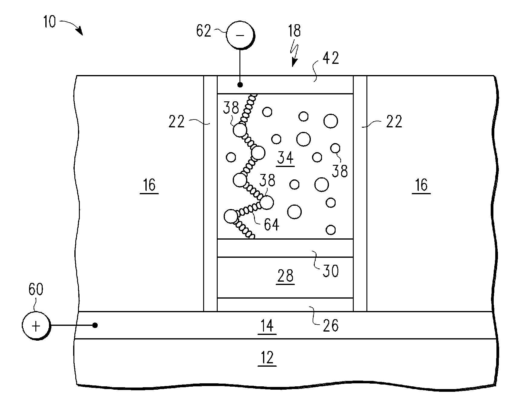
[0013]According to one embodiment of the method of the present disclosure, conductive bridge random access memory (CBRAM) devices are formed with use of selective deposition of silver (Ag) in contrast to sputter deposition. In one embodiment, the Ag is deposited by a selective displacement process. In addition, the method includes the formation of a selectively deposited diffusion control layer on the silver. In one embodiment, the diffusion control layer comprises, for example, cobalt (Co), tungsten (W), rhenium, or Molybdenum, and an additional element X (CoWX), where X includes one or more of boron (B), and phosphorus (P). Furthermore, the method of the present disclosure advantageously uses a barrier layer of CoWX for controlling diffusion of Ag within the CBRAM. The barrier layer of CoWX also possesses a thickness dependent barrier property, in which a desired barrier property can be controlled via the barrier layer thickness according to the requirements of a given CBRAM appli...


PUM


Abstract

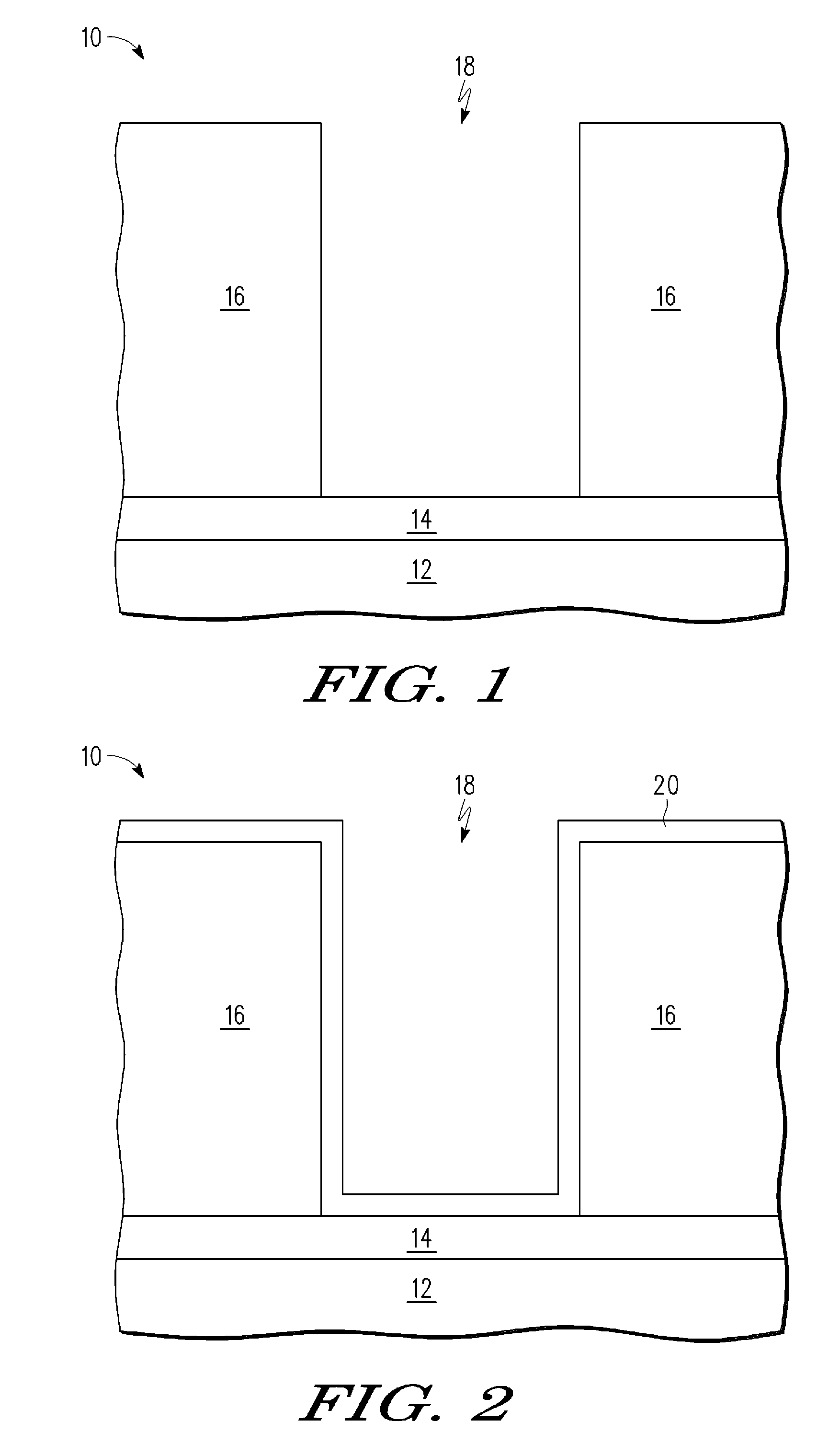
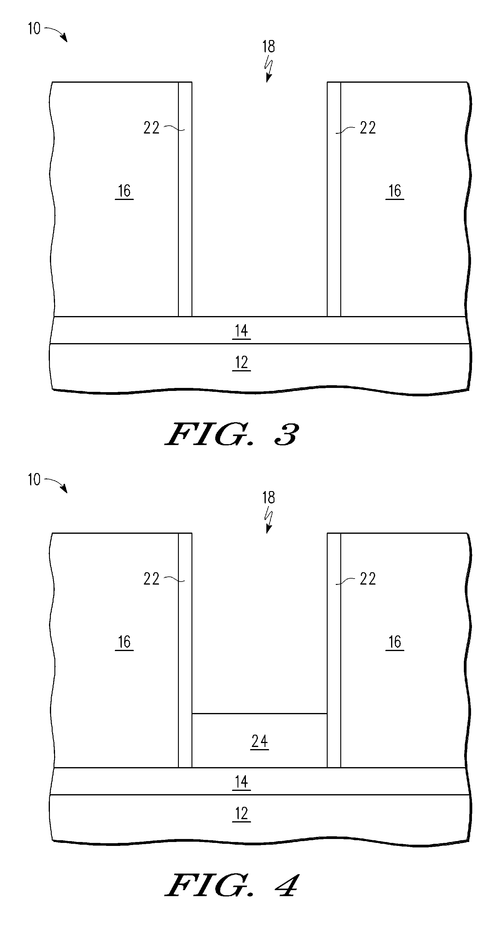
A method for making a semiconductor device (10) includes providing an interconnect layer (14) over an underlying layer (12), forming a first insulating layer (16) over the interconnect layer, and forming an opening (18) through the insulating layer to the interconnect layer. A first conductive layer (24) is formed over the interconnect layer and in the opening. This is performed by plating so it is selective. A second conductive layer (28) in the opening is formed by displacement by immersion. This is performed after the first conductive layer has been formed. The result is the second conductive layer is formed by a selective deposition and is effective for providing it with bridging material. A layer of bridgeable material (34) is formed over the second conductive layer and in the opening. A third conductive layer (42) is formed over the bridgeable material. The semiconductor device may be useable as a conductive bridge memory device.

Description

BACKGROUND[0001]1. Field[0002]This disclosure relates generally to semiconductor memory devices, and more specifically, to conductive bridge random access memory devices and methods of making the same.[0003]2. Related Art[0004]Programmable metallization memories, also referred to as conductive bridge random access memory (CBRAM) cells, generally consist of a chalcogenide material / silver diffusion layer that is sandwiched between a bottom electrode (e.g. W) and an upper electrode (Ag or Cu). Memory cell operation is believed to be due to formation / dissolution of a conductive bridge formed by electro-deposition of silver. It is important to have diffusion of silver ions to chalcogenide occur in a controllable manner. However, in the current known fabrication method for CBRAM cells, silver is deposited by a physical vapor deposition (PVD) process. In such a method, silver diffuses rapidly into the chalcogenide during the PVD step itself and thus the silver diffusion is largely uncontro...

Claims


Application Information

Patent Timeline
Patent Type & Authority Applications(United States)
IPC IPC(8): H01L21/441H01L29/04
CPCH01L45/085H01L45/1233H01L45/1253H01L45/1658H01L45/1683H01L45/142H01L45/143H01L45/1266H10N70/245H10N70/8416H10N70/841H10N70/8822H10N70/8825H10N70/046H10N70/826H10N70/066
Inventor MATHEW, VARUGHESEGARCIA, SAM S.MERCHANT, TUSHAR P.
Owner NXP USA INC
Learn More