

Voltage multiplier with improved efficiency
a voltage multiplier and efficiency technology, applied in the field of integrated circuits, can solve problems such as reducing the amount of charge transferred, affecting the output voltage of the voltage multiplier circuit, and reducing the threshold voltag
- Summary
- Abstract
- Description
- Claims
- Application Information
AI Technical Summary
Problems solved by technology
Method used
Image

Examples
Embodiment Construction
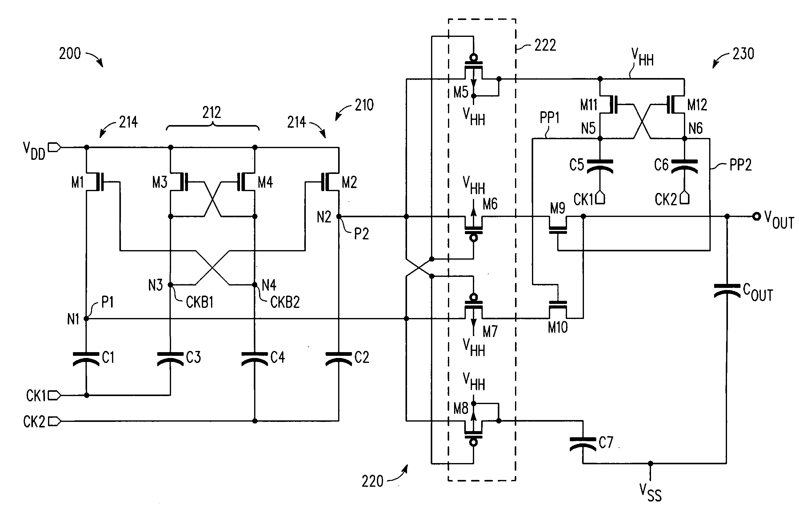
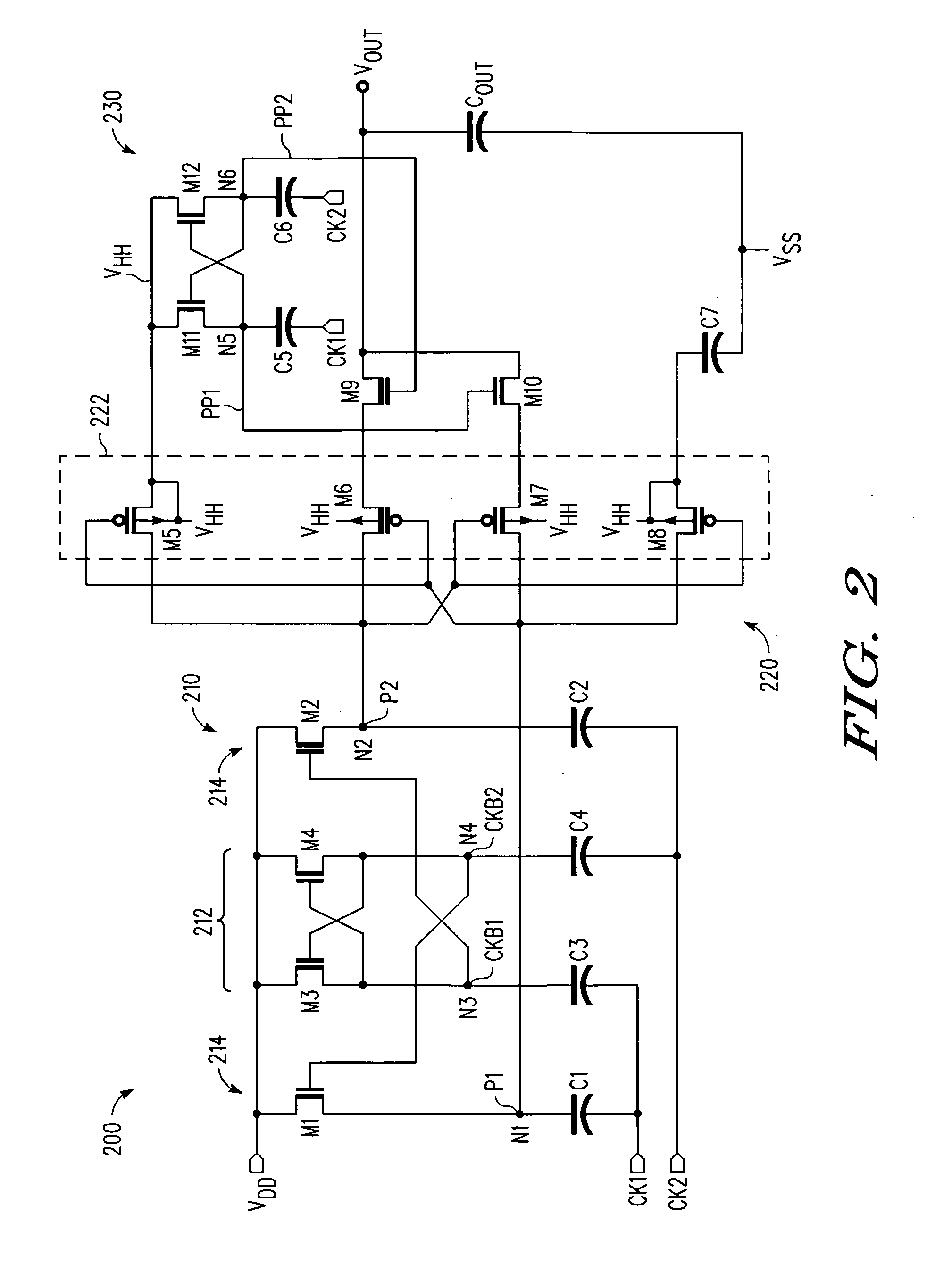
[0014]A multi-stage voltage multiplication circuit and methodology are described for use in integrated circuit applications to efficiently develop an output voltage that is higher than the input supply voltage. In selected embodiments, a two-stage complementary switch is used to connect boosted clock signals from a charge pump to the multiplier output in which the complementary switches are separately clocked. With the two-stage complementary switch, return current from the storage capacitor to the pumping capacitor is blocked, thereby increasing power transfer efficiency, even at high clock frequencies when clock skews are particularly harmful to converter efficiency. In general terms, the multi-stage voltage multiplier circuit includes a booster circuit that is clocked by non-overlapping clock inputs, and a pass gate circuit that selectively couples the booster circuit to the voltage multiplier output while preventing current return. The booster circuit may be implemented with two...
PUM
 Abstract
Description
Claims
Application Information