LED chip package structure applied to a backlight module and method for making the same

a backlight module and chip package technology, applied in the field of led, can solve the problems of time-consuming known packaging process known led package structure does not offer a good display for users, etc., and achieve the effect of less time and simple process for led chip package structur

Inactive Publication Date: 2009-09-10
HARVATEK CORPORATION
View PDF11 Cites 16 Cited by
  • Summary
  • Abstract
  • Description
  • Claims
  • Application Information

AI Technical Summary

Benefits of technology

[0006]The present invention provides an LED chip package structure applied to a backlight module and a method for making the same. When the LED chip package structure of the present invention lights up, the LED chip package structure generates a series of light-generating areas on a body unit. Because the series of light-generating areas is continuous, no dark bands are produced between two adjacent LED chips. Furthermore, because the LED chips are arranged on a substrate body via a COB (Chip On Board) method and a hot pressing method, the process for the LED chip package structure is simple and less time is needed for the manufacturing process. Furthermore, the LED chip package structure can be applied to any type of light source such as a back light module, a decorative lamp, a lighting lamp, or a scanner.

Problems solved by technology

Hence, the known packaging process is time-consuming.
Hence, the known LED package structure does not offer a good display for users.

Method used


Image

  • LED chip package structure applied to a backlight module and method for making the same
  • LED chip package structure applied to a backlight module and method for making the same
  • LED chip package structure applied to a backlight module and method for making the same

Examples


first embodiment

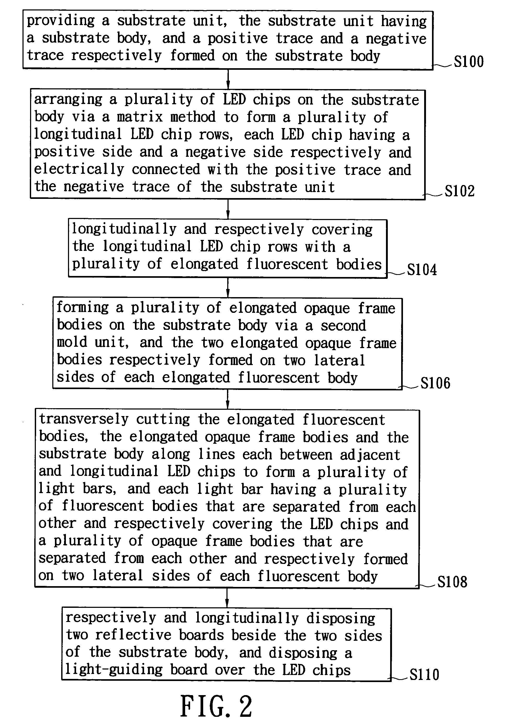
[0023]Referring to FIGS. 2, 2a to 2e, and 2A to 2E, the present invention provides a method for making an LED chip package structure applied to a backlight module. The method includes: referring to FIGS. 2a and 2A, providing a substrate unit 1, the substrate unit having a substrate body 10, and a positive trace 11 and a negative trace 12 respectively formed on the substrate body 10 (S100).

[0024]Moreover, the substrate body 10 has a metal layer 10A and a Bakelite layer 10B formed on the metal layer 10A. The substrate unit 1 can be a PCB (Printed Circuit Board), a flexible substrate, an aluminum substrate, a ceramic substrate, or a copper substrate according to different needs. In addition, both the positive trace 11 and the negative trace 12 can be aluminum circuits or silver circuits. The layouts of the positive trace 11 and the negative trace 12 are determined by different needs.

[0025]Referring to FIGS. 2b and 2B, the method of the first embodiment further includes: arranging a plu...

second embodiment

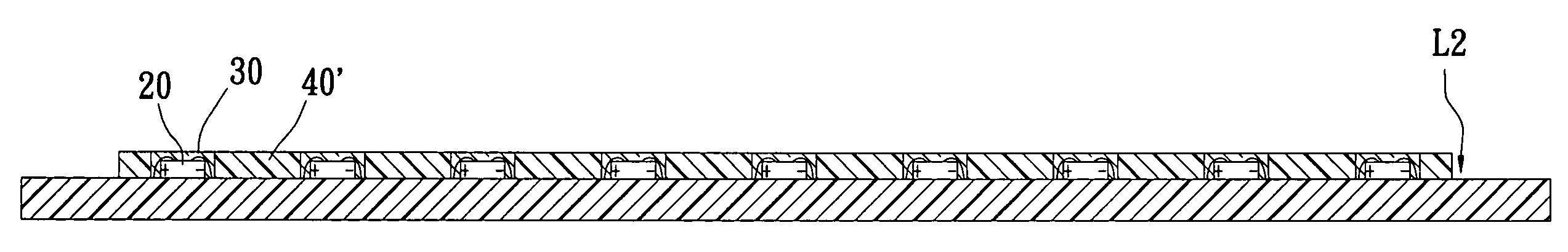
[0032]Finally, referring to FIGS. 2d, 2e, and 2E, the method of the second embodiment further includes: transversely cutting the elongated fluorescent bodies 3, the elongated opaque frame bodies 4 and the substrate body 10 along lines each between adjacent and longitudinal LED chips 20 to form a plurality of light bars L1, and each light bar L1 having a plurality of fluorescent bodies 30 that are separated from each other and respectively covering the LED chips 20 and a plurality of opaque frame bodies 40 that are separated from each other and respectively formed on two lateral sides of each fluorescent body 30 (S108). Moreover, the longitudinal width of each fluorescent body 30 and each opaque frame body 40 is below 0.3 mm, such as between 0.01 mm and 0.3 mm.

[0033]Referring to FIGS. 4A and 4B, the first embodiment of the present invention further includes: respectively and longitudinally disposing two reflective boards 5 beside the two sides of the substrate body 10, and disposing ...


PUM


Abstract

An LED chip package structure applied to a backlight module includes a substrate unit, a light-emitting unit, a package body unit and an opaque unit. The light-emitting unit has a plurality of LED chips electrically arranged on the substrate unit. The package body unit has a plurality of package bodies respectively covering the LED chips. The opaque unit has a plurality of opaque frame bodies formed on the substrate unit, and two opaque frame bodies are respectively formed on two lateral sides of each package body.

Description

BACKGROUND OF THE INVENTION[0001]1. Field of The Invention[0002]The present invention relates to an LED chip package structure and a method for making the same, and particularly relates to an LED chip package structure applied to a backlight module and a method for making the same.[0003]2. Description of the Related Art[0004]Referring to FIG. 1, a known method for packaging LED chips is shown. The known method includes: providing a plurality of packaged LEDs that have been packaged (S800); providing an elongated substrate body that has a positive trace and a negative trace (S802); and then, arranging each packaged LED on the elongated substrate body in sequence and electrically connecting a positive side and a negative side of each packaged LED with the positive trace and the negative trace of the substrate body (S804).[0005]However, with regard to the known method, each packaged LED needs to be firstly cut from an entire LED package structure, and then each packaged LED is arranged...

Claims


Application Information

Patent Timeline
Patent Type & Authority Applications(United States)
IPC IPC(8): H01L33/00H01L21/50
CPCF21K9/00G02B6/0068G02B6/0073F21Y2103/003G02F1/133603F21K9/30G02B6/0083F21K9/20F21Y2103/10F21Y2115/10H01L2224/48091H01L2924/00014
Inventor WANG, BILYWU, SHIH-YUWU, WEN-KUEI
Owner HARVATEK CORPORATION
Why Eureka
Try Eureka