Substrate strip for semiconductor packages

a technology of substrate strips and semiconductors, applied in the direction of semiconductor devices, semiconductor/solid-state device details, electrical apparatus, etc., can solve the problems of chip damage, cracks on the side rails of substrate strips, and damage to electronic devices such as chips disposed on packaging units, so as to reduce moisture penetration, improve stress distribution, and slow crack growth

Inactive Publication Date: 2009-09-10
POWERTECH TECHNOLOGY
View PDF4 Cites 17 Cited by
  • Summary
  • Abstract
  • Description
  • Claims
  • Application Information

AI Technical Summary

Benefits of technology

[0003]The main purpose of the present invention is to provide a substrate strip for semiconductor packages to slow crack growth b

Problems solved by technology

During handling and transporting of the semiconductor packaging processes, cracks will form on the side rails of the substrate strip due to stresses and friction.
Moreover, the cracks

Method used


Image

  • Substrate strip for semiconductor packages
  • Substrate strip for semiconductor packages
  • Substrate strip for semiconductor packages

Examples


first embodiment

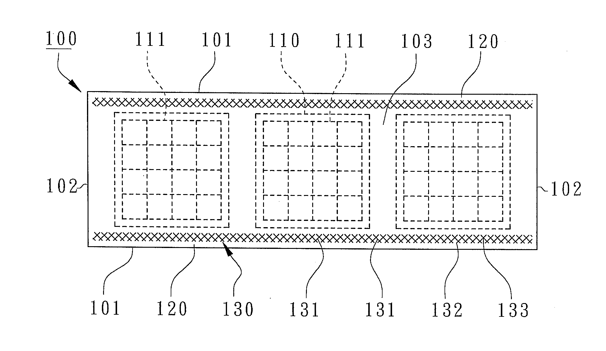
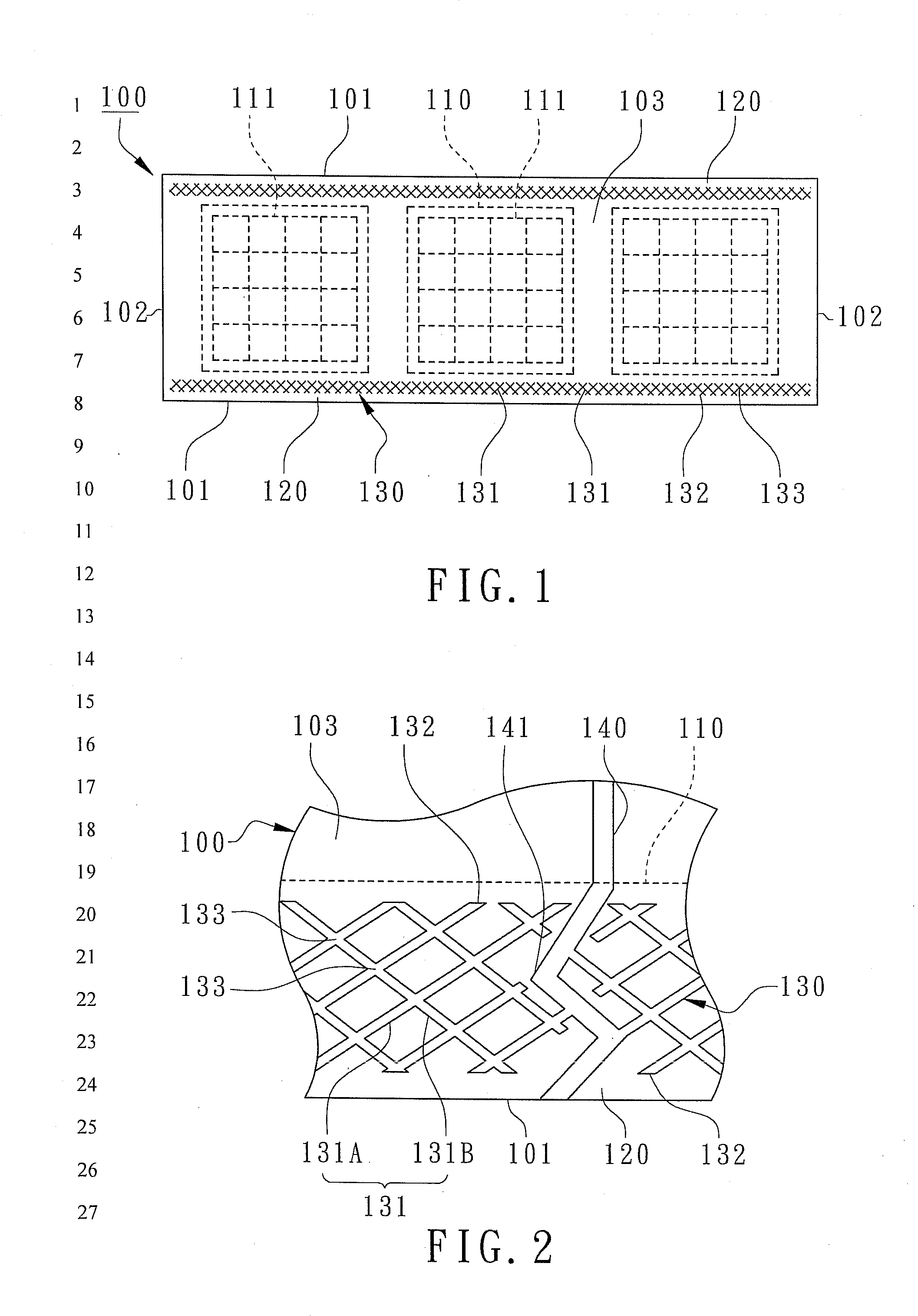
[0013]According to the present invention, as shown in FIG. 1 to FIG. 3, a substrate strip for semiconductor packages is revealed. As shown in FIG. 1, a substrate strip 100 for semiconductor packages primarily comprises at least a molding area 110 and two side rails 120. The substrate strip 100 has two opposing longer sides 101 and two opposing shorter sides 102 perpendicular to the two opposing longer sides 101 where the lengths of the longer sides 101 are two times longer than the ones of the shorter sides 102, generally at least twice the lengths. To be more specific, as shown in FIG. 3, the substrate strip 100 further has a top surface 103 and a bottom surface 104. The molding area 110 has a circuit layer formed on the top surface 103, not shown in the figure. Normally, the substrate strip 100 can be a single-layer, a double-layer, or a multi-layer printed circuit board.

[0014]The molding area 110 includes a plurality of packaging units 111. The packaging units 111 mean the chip c...

second embodiment

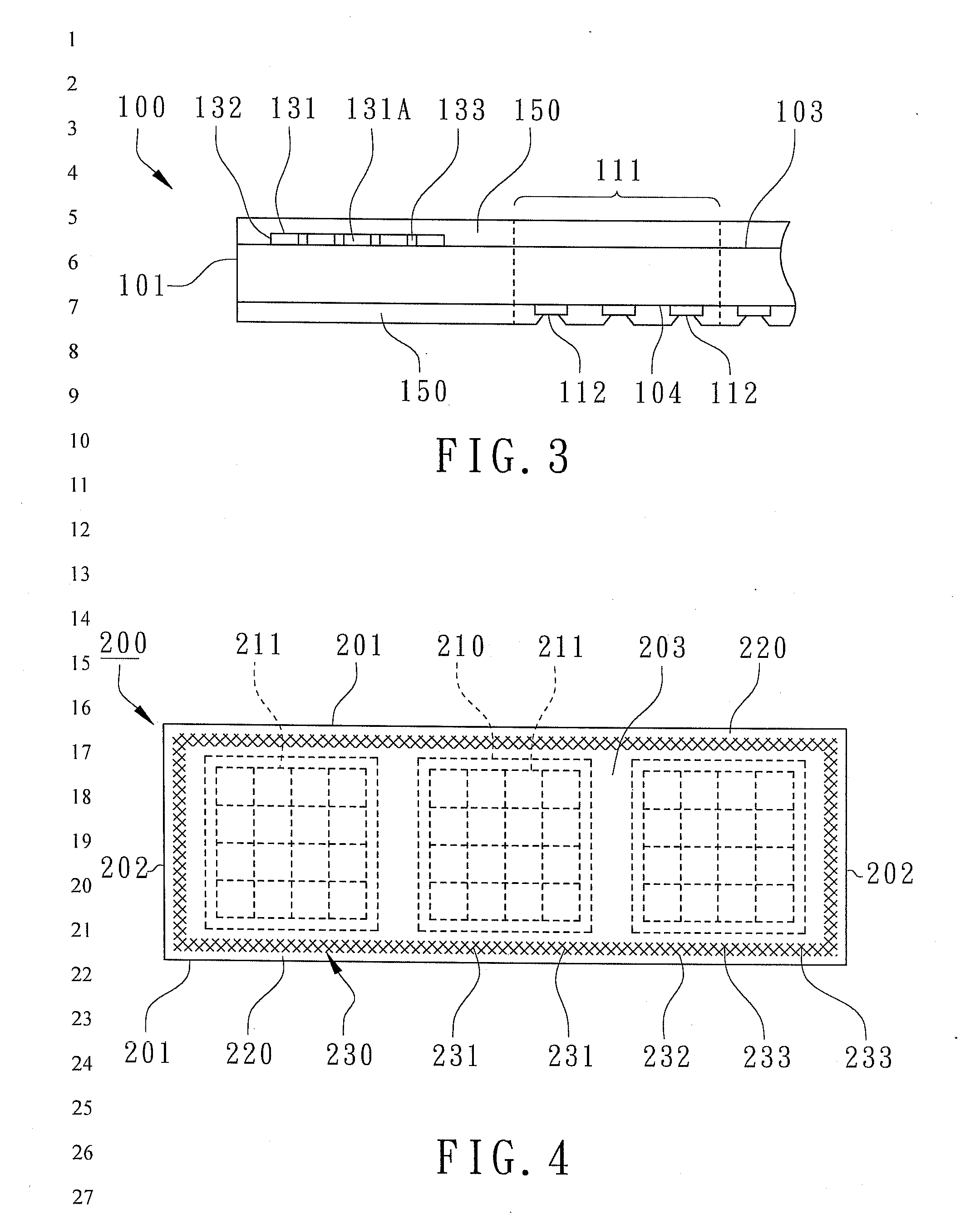
[0019]The numbers and the locations of metal meshes in the present invention are not limited. In the present invention, as shown in FIG. 4, another substrate strip 200 for semiconductor packages is revealed, primarily comprising at least a molding area 210 and two side rails 220. The molding area 210 includes a plurality of packaging units 211. The side rails 220 are located outside the molding area 210 and include two opposing loner sides 201 of the substrate strip 200. A metal mesh 230 is disposed on the side rails 220. The metal mesh 230 consists of a plurality of crisscrossed wires 231 having a plurality of isolated wire terminals 232 located at one edge of the metal mesh 230. The crisscrossed wires 231 are mutually interlaced to each other formed a plurality of intersections 233. Accordingly, the specific metal mesh 230 is configured to slow the growth of cracks. As shown in FIG. 4 again, in the present embodiment, the metal mesh 230 is further disposed on the other peripheries...


PUM


Abstract

A substrate strip for semiconductor packages to slow the crack growth, primarily comprises a molding area and two side rails. The molding area includes a plurality of packaging units. The side rails are located outside the molding area and include two opposing longer sides of the substrate strip. A metal mesh is disposed on the side rails. The metal mesh consists of a plurality of crisscrossed wires having a plurality of isolated wire terminals at one edge of the metal mesh. Accordingly, crack growth is slowed by the specific metal mesh without damaging the packaging units. In one embodiment, the metal mesh is without boundary wires connecting to the isolated wire terminals to enhance the resistance to crack growth.

Description

FIELD OF THE INVENTION[0001]The present invention relates to a printed circuit board, especially to a substrate strip for semiconductor packages to slow the growth of cracks.BACKGROUND OF THE INVENTION[0002]In the conventional semiconductor packaging processes, a substrate strip is used as a chip carrier for mounting a plurality of chips to meet the requirements of lower cost and mass production. The molding area on the substrate strip includes a plurality of packaging units arranged in an array. After semiconductor packaging processes such as die attachment, electrical connections, and molding, the substrate strip is singulated along the scribe lines between the package units to form a plurality of semiconductor packages. During handling and transporting of the semiconductor packaging processes, cracks will form on the side rails of the substrate strip due to stresses and friction. Moreover, the cracks grow due to more exerted stresses and extend into the molding area of the packag...

Claims


Application Information

Patent Timeline
IPC IPC(8): H01L23/48
CPCH01L23/13H01L23/49838H01L2924/01079H01L2924/01078H01L24/97
Inventor FAN, WEN-JENG
Owner POWERTECH TECHNOLOGY
Why Eureka
Try Eureka