Semiconductor device and method of manufacturing the same

a technology of semiconductor devices and semiconductor chips, applied in semiconductor devices, semiconductor/solid-state device details, electrical devices, etc., can solve problems such as complicated process, leakage between the back side of the semiconductor chip and the casing, and complicated process

Inactive Publication Date: 2009-09-10
DENSO CORP
View PDF5 Cites 29 Cited by
  • Summary
  • Abstract
  • Description
  • Claims
  • Application Information

AI Technical Summary

Benefits of technology

[0009]According to the above method, it is possible to simplify a process of forming an insulating layer for insulating a heat sink and a casing from each other.
[0011]According to the above method, it is possible to simplify a process of forming an insulating layer for insulating a heat sink and a casing from each other.
[0013]According to the above method, it is possible to simplify a process of forming an insulating layer for insulating a heat sink and a casing from each other.
[0015]According to the above method, it is possible to simplify a process of forming an insulating layer for insulating a heat sink and a casing from each other.
[0017]According to the above method, it is possible to simplify a process of forming an insulating layer for insulating a heat sink and a casing from each other.
[0019]According to the above semiconductor device, it is possible to ensure insulation from the semiconductor chip from the casing.

Problems solved by technology

In such a case, there may generate a leak between a back side of the semiconductor chip and the casing.
Thus, a process of forming the insulating layer becomes complicated.
When an insulating film is placed between the heat sink and the casing, it is required to place the insulating film every time when the semiconductor chip and the heat sink are fixed to the casing, which results in a complicated process.

Method used


Image

  • Semiconductor device and method of manufacturing the same
  • Semiconductor device and method of manufacturing the same
  • Semiconductor device and method of manufacturing the same

Examples


first embodiment

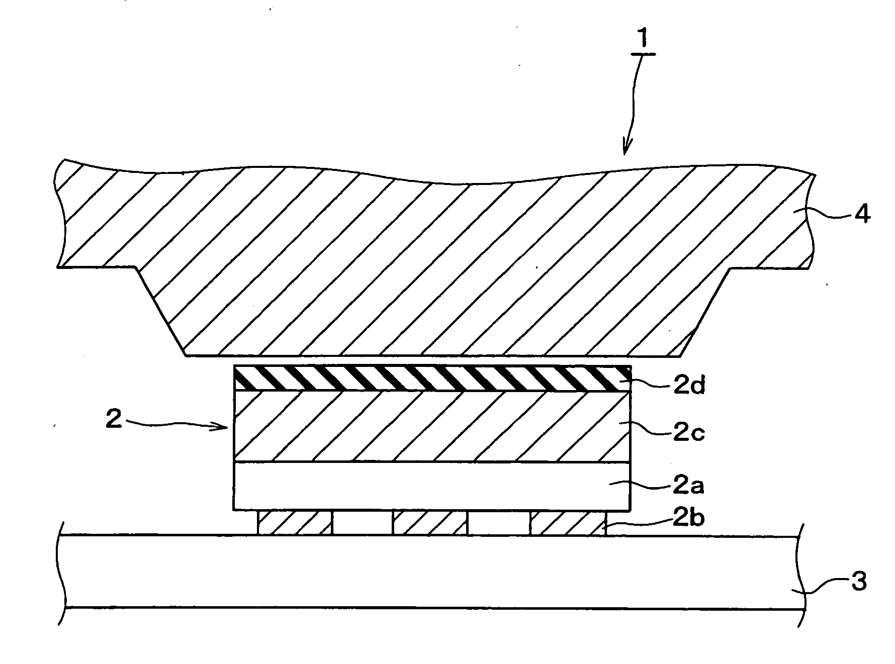
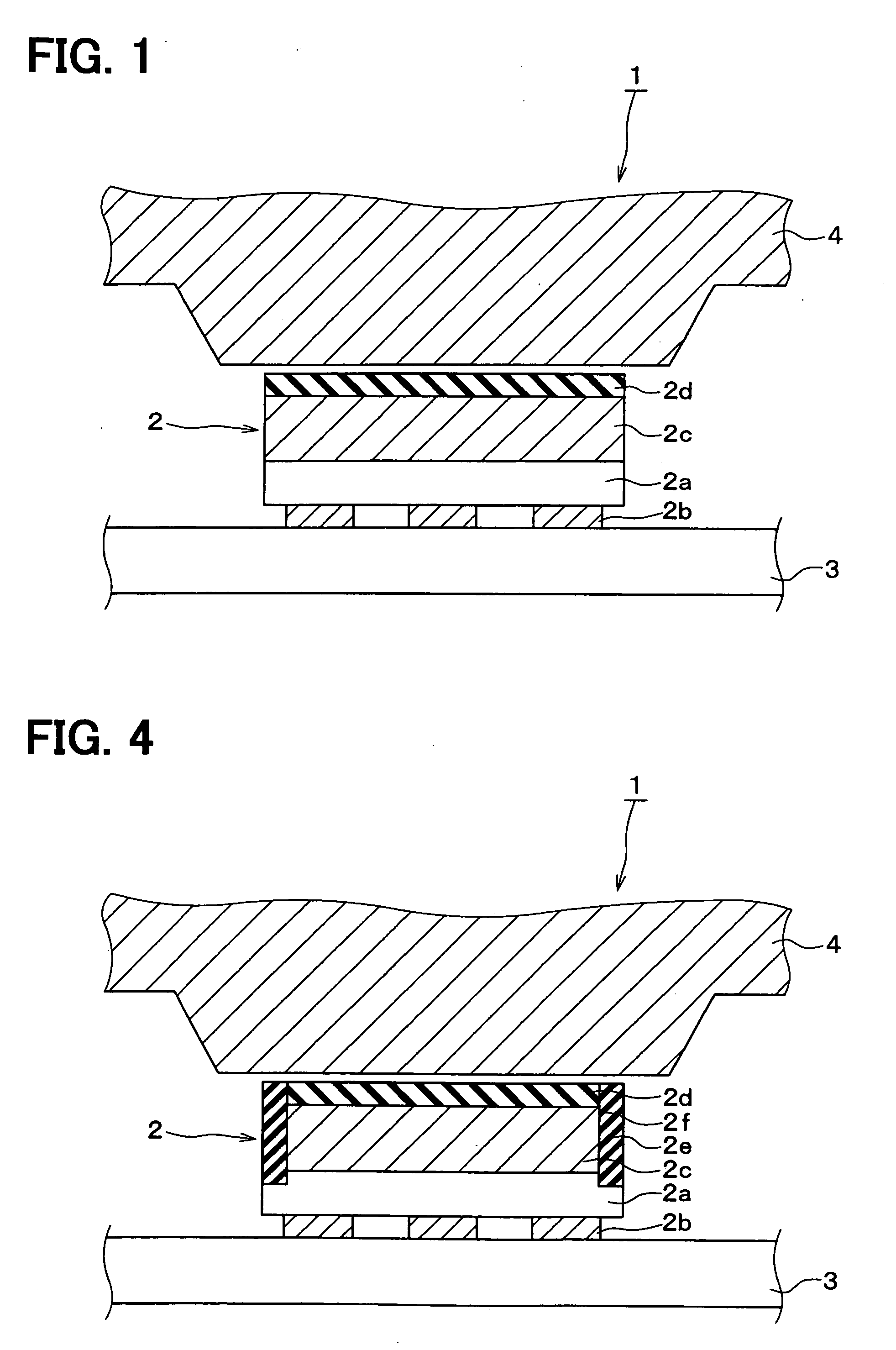
[0043]A first embodiment is described below. FIG. 1 is a cross sectional diagram illustrating a semiconductor device 1 in accordance with a first embodiment.

[0044]The semiconductor device 1 includes parts illustrated in, for example, FIG. 1 as a portion of the semiconductor device 1. The semiconductor device 1 may correspond to, for example, a power package having a power device, a central processing unit (CPU) generating a large amount of heat, or a passive device generating a large amount of heat. Alternatively, the semiconductor device 1 may correspond to a power unit having an element in addition to the above power package. Alternatively, the semiconductor device 1 may correspond to an electronic control unit (ECU) having a circuit or the like in addition to the above power package.

[0045]As shown in FIG. 1, the semiconductor device 1 includes a semiconductor chip 2, a board 3 (i.e., a printed circuit board) and a casing 4.

[0046]The semiconductor chip 2 includes an element part 2...

second embodiment

[0063]In a first embodiment, the heat sink 2c is exposed from an end face of the semiconductor chip 2. When working voltages of a semiconductor element are less than or equal to 60 V for instance, a configuration of a first embodiment can sufficiently ensure insulation of the heat sink 2c or the element part 2a from the casing 4 by means of grounding the casing 4 or the like. However, since the heat sink 2c is conductor, when a semiconductor element in the semiconductor chip 2 operates at high voltages, the presence of a thin insulating layer 2d only is difficult to ensure the insulation of the heat sink 2c or the element part 2a from the casing 4. Taking into account semiconductor devices used in high voltages, the present embodiment presents a configuration for enhancing the insulation of the heat sink 2c or the element part 2a from the casing 4.

[0064]FIG. 4 is a cross sectional diagram illustrating a semiconductor device 1 in accordance with the present embodiment. FIG. 5 is a la...

third embodiment

[0074]In the present embodiment, a method is presented below for manufacturing a configuration for insulation of the heat sink 2c or the element part 2a from the casing 4.

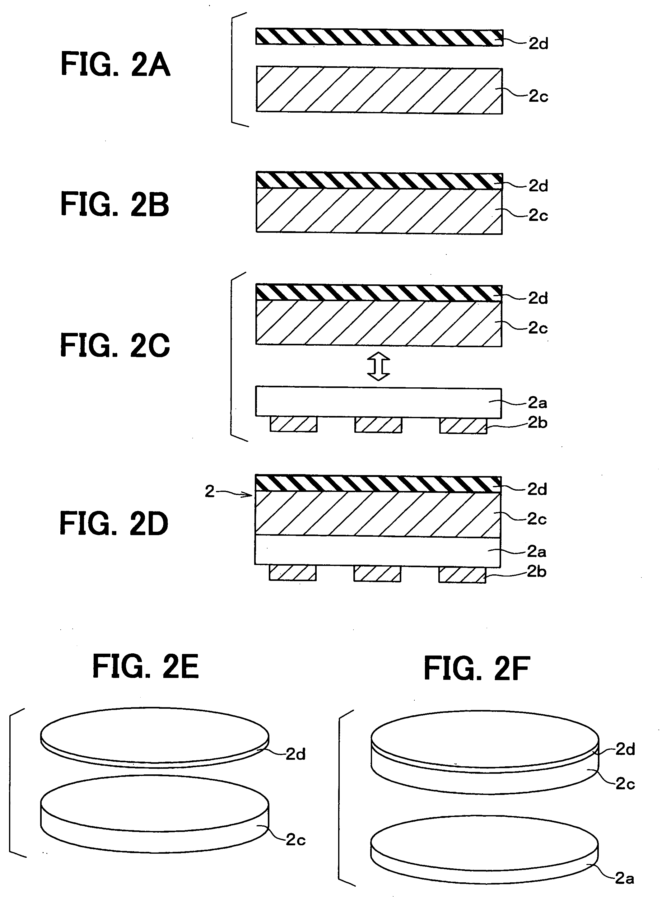
[0075]FIGS. 8A to 8D are cross sectional diagrams each illustrating a manufacturing process of a semiconductor chip 2 for a semiconductor device 1. Manufacturing processes of a semiconductor chip 2 of the present embodiment are generally similar to those of the first embodiment. Difference includes those shown in FIGS. 8A to 8D.

[0076]In a process exemplified in FIG. 8A, the processes exemplified in FIGS. 2A to 2D according to the first embodiment are performed. That is, a structure is formed in which a heat sink 2c and an insulating layer 2d are located on a rear surface side of a semiconductor wafer that a semiconductor element has been formed in. Then, a support member 6 is bonded to the electrode part 2b and the front surface of the semiconductor wafer, so that the semiconductor wafer, the heat sink 2c and the i...


PUM


Abstract

A semiconductor device and a method of manufacturing the same are disclosed. The semiconductor device includes: a casing, a board and a semiconductor chip. The chip includes: an element part; a heat sink bonded to the element part; an insulting layer located on the heat sink so that the heat sink is located between the element part and the insulating layer; and a side wall insulating layer covering all of end faces of the heat sink. The semiconductor chip is located between the casing and the board, so that the insulating layer is directed to the casing to enable heat radiation from the heat sink toward the casing via the insulating layer.

Description

CROSS REFERENCE TO RELATED APPLICATION[0001]The present application is based on Japanese Patent Applications No. 2008-57480 filed on Mar. 7, 2008 and No. 2008-288656 filed on Nov. 11, 2008, the disclosures of which are incorporated herein by reference.BACKGROUND OF THE INVENTION[0002]1. Field of the Invention[0003]The present invention relates to a semiconductor device having a configuration for heat radiation from a semiconductor chip to a casing. The present invention also relates to a method for manufacturing such a semiconductor device.[0004]2. Description of Related Art[0005]There is known a semiconductor device that has a face-down mounting structure. In a typical face-down mounting structure, an electrode is located on one surface of a semiconductor chip, and is electrically connected to a wiring pattern of a board with the one surface of the semiconductor chip being directed to the board. For improvement of heat radiation efficiency from a semiconductor chip having a face-do...

Claims


Application Information

Patent Timeline
Patent Type & Authority Applications(United States)
IPC IPC(8): H01L21/50
CPCH01L21/561H01L21/568H01L2924/1305H01L2924/014H01L2924/01074H01L21/6836H01L21/78H01L23/3114H01L23/3135H01L23/367H01L23/4334H01L24/16H01L24/94H01L2221/68377H01L2224/16225H01L2224/73253H01L2924/01029H01L2924/10253H01L2924/13055H01L2924/13091H01L2924/01005H01L2924/01006H01L2924/01023H01L2924/01033H01L2924/00H01L2924/15787H01L2224/04105
Inventor MIYAJIMA, TAKESHI
Owner DENSO CORP
Why Eureka
Try Eureka