Piezoelectric device and electronic apparatus

a piezoelectric device and electronic device technology, applied in piezoelectric/electrostrictive devices, piezoelectric/electrostrictive/magnetostrictive devices, semiconductor/solid-state device details, etc., can solve the problems of limiting the versatility of ic chip use, the piezoelectric device cannot be thin, and the piezoelectric device has a large planar size, so as to reduce the thickness of the piezoelectric device, the effect of thin

Active Publication Date: 2009-09-17
SEIKO EPSON CORP
View PDF3 Cites 19 Cited by
  • Summary
  • Abstract
  • Description
  • Claims
  • Application Information

AI Technical Summary

Benefits of technology

[0008]An advantage of the present invention is to provide a thin piezoelectric device and an electronic apparatus having such piezoelectric device.
[0009]A piezoelectric device according to one aspect of the invention includes an integrated circuit (IC) chip and a piezoelectric resonator element, a part of the piezoelectric resonator element being disposed so as to overlap with a part of the IC chip when viewed in plan. The IC chip includes an inner pad disposed on an active face and in an area where is overlapped with the piezoelectric resonator when viewed in plan, an insulating layer formed on the active face, a relocation pad disposed on the insulating layer and in an area other than a part where is overlapped with the piezoelectric resonator element, the relocation pad being coupled to an end part of a first wire, and a second wire electrically coupling the inner pad and the relocation pad, the second wire having a relocation wire and a connector that penetrates the insulating layer, the relocation wire being disposed between the insulating layer and the active face.
[0010]According to the aspect of the invention, the location of the pad can be freely changed through the relocation wire, the connector, the relocation pad and the insulating layer. When the piezoelectric resonator element is arranged at the same position as the IC chip when they are viewed in plan, the relocation pad can be disposed in this area where the piezoelectric resonator element does not overlap with the IC chip irrespective of the position of the pad which is provided on one face of the IC chip. In this arrangement, the first wire can be extended from the relocation pad to the position adjacent to the piezoelectric resonator element, in other words, the first wire will not be provided between the piezoelectric resonator element and the IC chip. In this way, it is possible to reduce the thickness of the piez

Problems solved by technology

However, when the gap between the piezoelectric resonator element and the wire is wide, it is impossible to make the piezoelectric device thin.
In case of the piezoelectric device in which the longer side of the piezoelectric resonator element is arranged so as to cross over the longer side of the IC chip when viewed in plan and the pad is disposed laterally to

Method used


Image

  • Piezoelectric device and electronic apparatus
  • Piezoelectric device and electronic apparatus
  • Piezoelectric device and electronic apparatus

Examples


Embodiment Construction

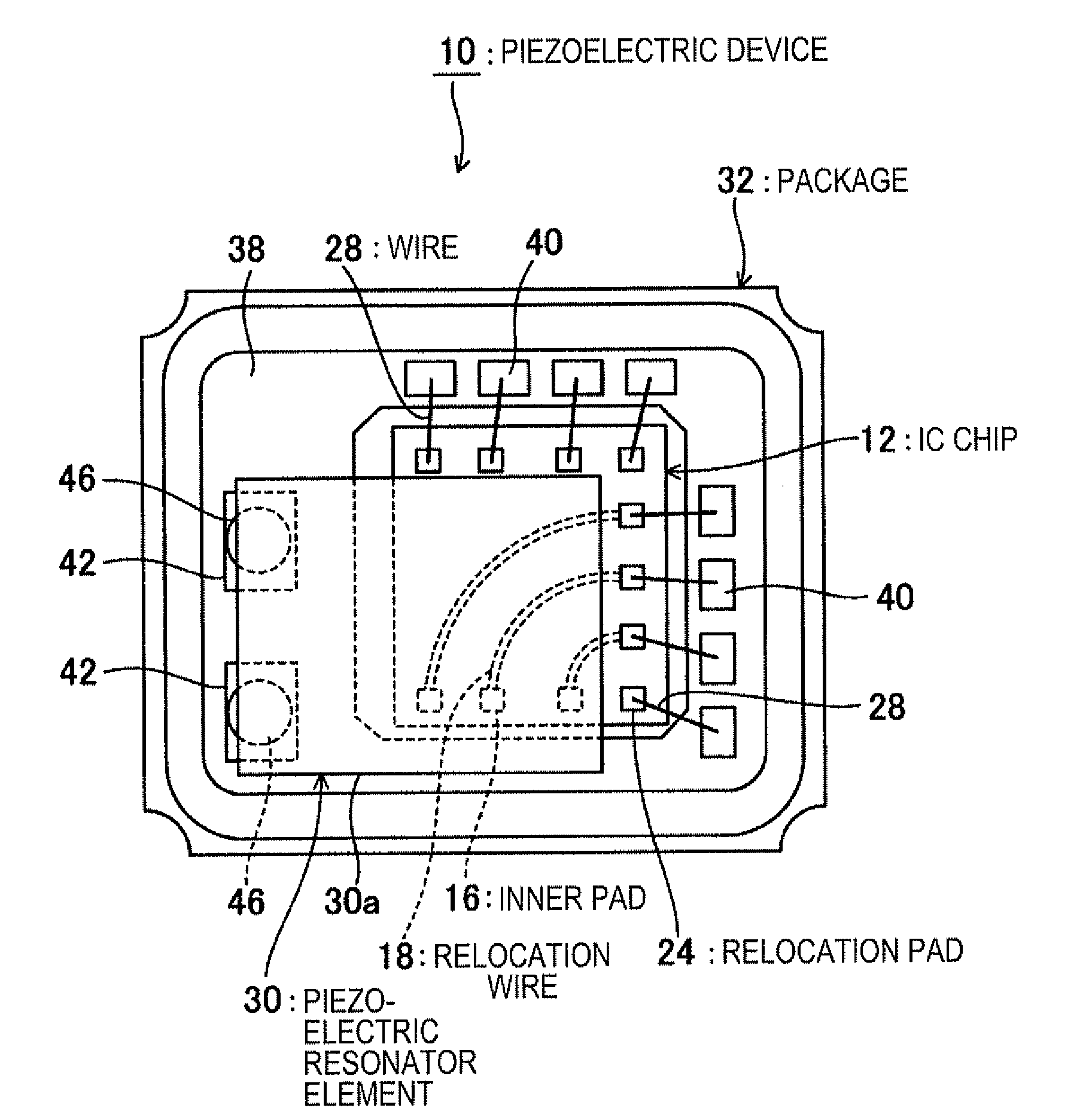
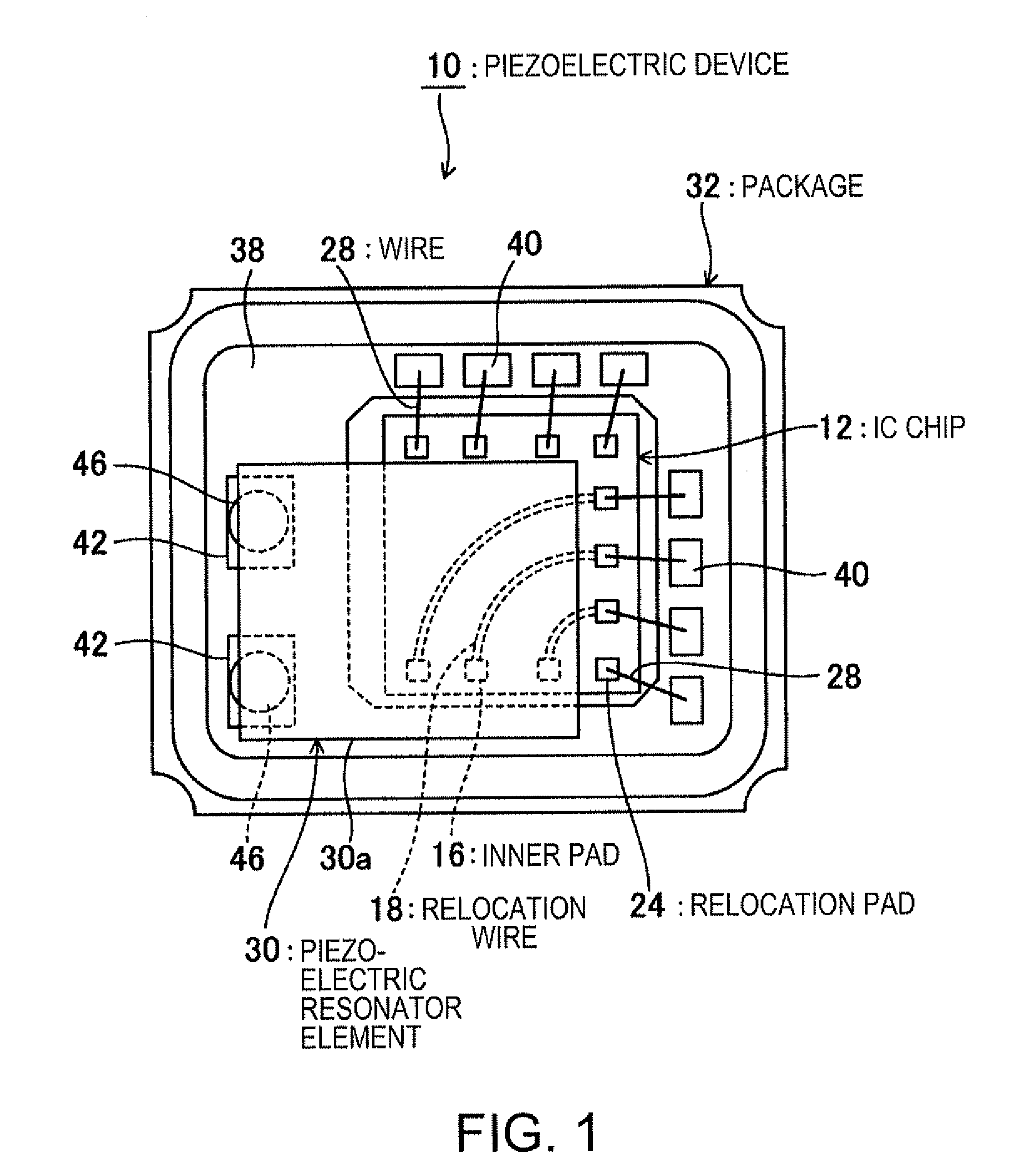
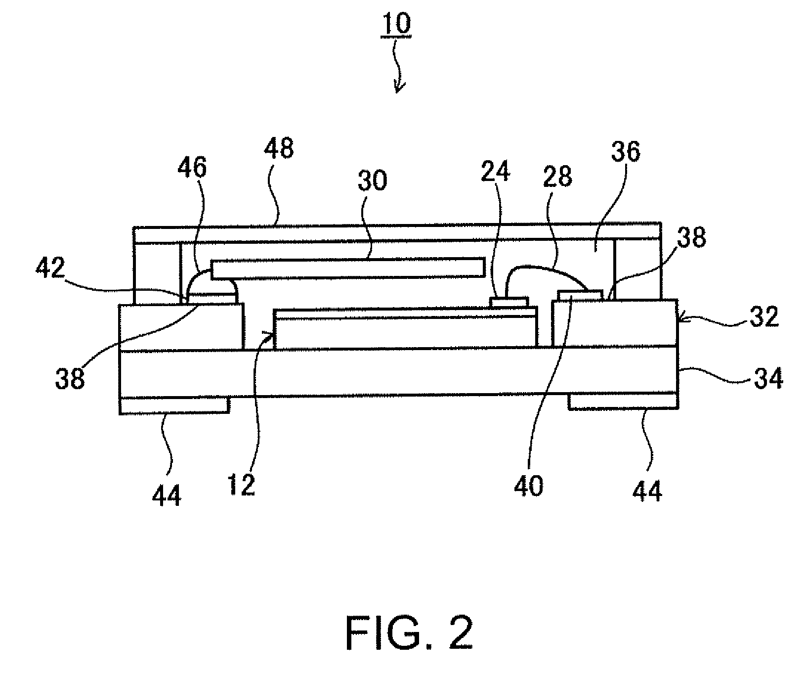
[0024]Embodiments of the invention will be described. FIG. 1 is a plan view of a piezoelectric device. FIG. 1 shows a state when a lid is removed from the device. FIG. 2 is a sectional view of the piezoelectric device. FIG. 3 is a schematic sectional view of an IC chip. FIGS. 4A and 4B are plan views of the IC chip showing an active face of a semiconductor element and a surface of an insulating layer.

[0025]Referring to FIG. 1 and FIG. 2, a piezoelectric device 10 includes an IC chip 12 and a piezoelectric resonator element 30 which are disposed in a layered direction and placed in a package 32. Referring to FIG. 3, the IC chip 12 includes a semiconductor element 14 in which a circuit is formed and an insulating layer 22 which is provided on an active face 14a (on one face) of the semiconductor element 14.

[0026]The semiconductor element 14 has a circuit (an oscillation circuit) that amplifies an electric signal which is inputted or outputted into / from the piezoelectric resonator elem...


PUM


Abstract

A piezoelectric device includes an integrated circuit (IC) chip and a piezoelectric resonator element, a part of the piezoelectric resonator element being disposed so as to overlap with a part of the IC chip when viewed in plan. The IC chip includes: an inner pad disposed on an active face and in an area where is overlapped with the piezoelectric resonator when viewed in plan; an insulating layer formed on the active face; a relocation pad disposed on the insulating layer and in an area other than a part where is overlapped with the piezoelectric resonator element, the relocation pad being coupled to an end part of a first wire; and a second wire electrically coupling the inner pad and the relocation pad, the second wire having a relocation wire and a connector that penetrates the insulating layer, the relocation wire being disposed between the insulating layer and the active face.

Description

BACKGROUND[0001]1. Technical Field[0002]The present invention relates to a piezoelectric device and an electronic apparatus, and more particularly relates to a piezoelectric device that has a piezoelectric resonator element and a circuit which oscillates the piezoelectric resonator element, and to an electronic apparatus having such piezoelectric device.[0003]2. Related Art[0004]There is a piezoelectric device having a piezoelectric resonator element and a circuit (an oscillation circuit) that is conductively coupled with the piezoelectric resonator element and oscillates the element in a package. JP-A-2004-15441 is a first example of related art. The oscillation circuit is an integrated circuit (IC) chip having an active face where a pad to which a wire is coupled is provided. According to the first example, the package includes a package base that has a concave portion whose opening faces upward and a lid that is placed onto an upper face of the package base and seals the concave ...

Claims


Application Information

Patent Timeline
IPC IPC(8): H01L23/485
CPCH03H9/0547H03H9/1021H01L41/0475H01L41/09H01L2224/48091H01L2224/05554H01L2924/00014H01L2924/16195H01L2224/023H01L2924/0001H10N30/875H10N30/20
Inventor SHIMODAIRA, KAZUHIKO
Owner SEIKO EPSON CORP
Why Eureka
Try Eureka