Display device, display device manufacturing method, substrate, and color filter substrate

a display device and manufacturing method technology, applied in non-linear optics, instruments, optics, etc., can solve the problems of lowering the alignment accuracy of substrates, gap deficiency, and lowering production efficiency, and achieve the effect of facilitating uv curing of sealants

Inactive Publication Date: 2009-09-17
SHARP KK
View PDF9 Cites 49 Cited by
  • Summary
  • Abstract
  • Description
  • Claims
  • Application Information

AI Technical Summary

Benefits of technology

[0047]As described above, the present invention can provide a display device, a display device manufacturing method, a substrate, and a color filter substrate which facilitate UV curing of a sealant.

Problems solved by technology

For this reason, the alignment accuracy of substrates lowers and gap deficiency caused due to line discontinuity or a dry spot of the sealant is caused.
Further, it takes about one hour to heat-cure the sealant, thereby involving lowering of the production efficiency.
The bonded substrates thus manufactured suppresses lowering of alignment accuracy of the substrates and gap deficiency caused due to line discontinuity and a dry spot of the sealant, when compared with that using a sealant of which main component is thermosetting epoxy resin.
In such substrate bonding by providing the sealant on the light shielding layer, however, the light shielding layer intercepts the irradiated UV ray to inhibit the UV ray from reaching the entire sealant, thereby leaving a part of the sealant uncured.
Further, for narrowing the frame edge of a panel using a TFT substrate including a driver at its light shielding part, it is difficult for the UV ray to reach the entire sealant because of the presence of the driver, thereby leaving a part of the sealant uncured, as well.

Method used


Image

  • Display device, display device manufacturing method, substrate, and color filter substrate
  • Display device, display device manufacturing method, substrate, and color filter substrate
  • Display device, display device manufacturing method, substrate, and color filter substrate

Examples


embodiment 1

[0087](Constructions of color filter substrate 11 and liquid crystal display device 10 using it)

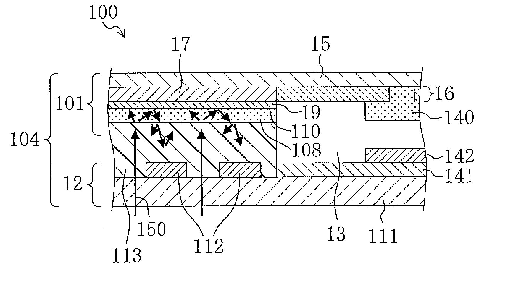
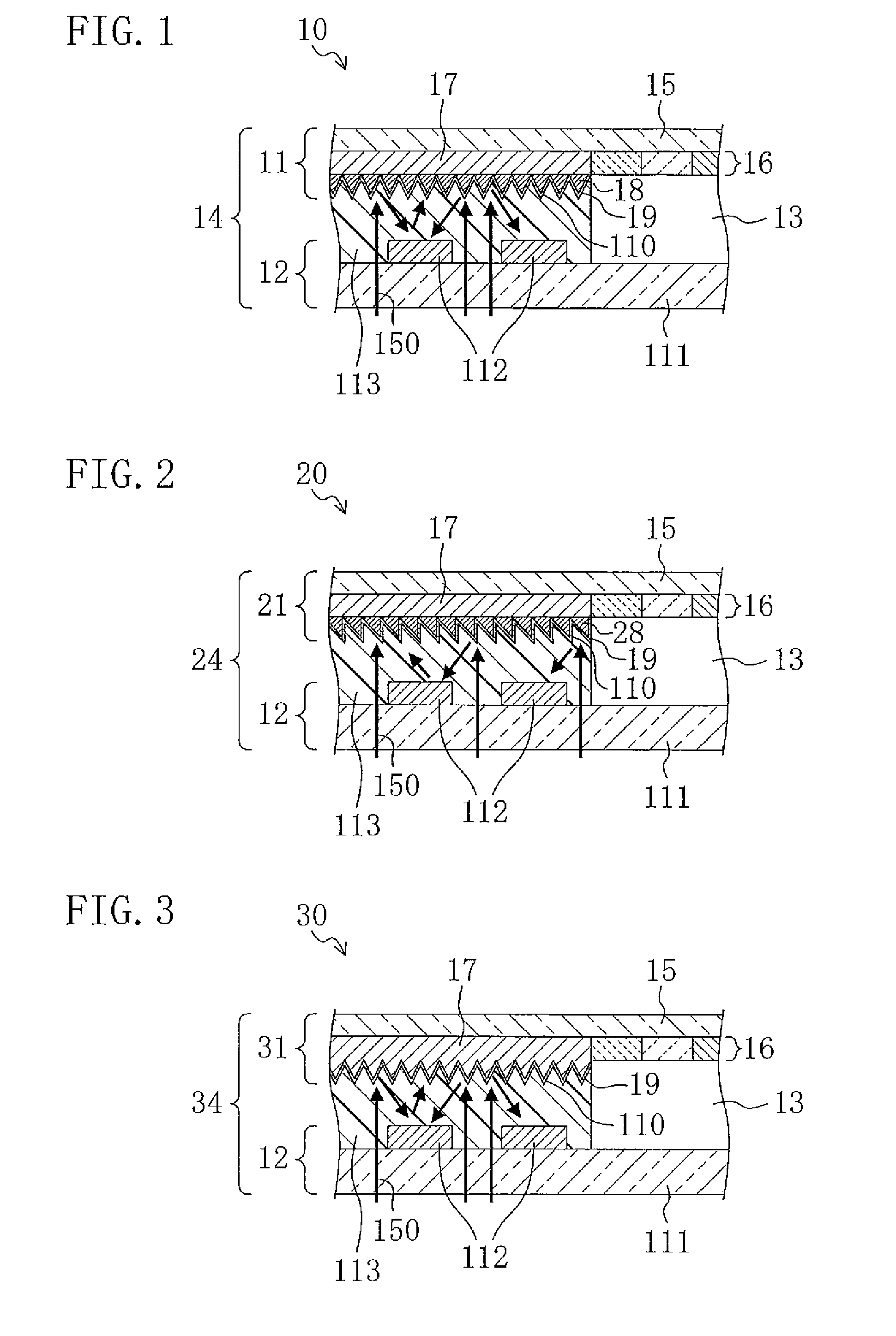
[0088]FIG. 1 is a sectional view of a liquid crystal display device 10. The liquid crystal display device 10 includes a liquid crystal display panel 14, a backlight unit (not shown), and the like, wherein the liquid display panel 14 includes a color filter substrate 11 and a thin film transistor substrate 12 which are opposed to each other, a liquid crystal layer 13 (display medium layer) provided therebetween, and column shaped spacers (not shown) provided between the opposed substrates.

[0089]In the color filter substrate (CF substrate 11), a color layer 16 of three primary colors of red (R), green (G), and blue (B) is formed on a glass substrate 15 to form a display part. The color layer 16 may include complementary colors of cyan, magenta, and yellow in addition to the combination of RGB.

[0090]A counter electrode and an alignment film (both not shown) are formed on the color layer 16. ...

embodiment 2

[0117](Constructions of Color Filter Substrate 21 and Liquid Crystal Display Device 20 Using it)

[0118]FIG. 2 is a sectional view of a liquid crystal display device 20 in accordance with Embodiment 2. The same reference numerals are assigned to the same parts as those indicated in the above embodiment for omitting description thereof.

[0119]The liquid crystal display device 20 includes a liquid crystal display panel 24, the back light, and the like (not shown), wherein the liquid crystal display panel 24 includes the TFT substrate 12 and a CF substrate 21 opposed to each other and the liquid crystal layer 13 between the substrates.

[0120]In the CF substrate 21, the color layer 16 composing the display part and the counter electrode and the alignment film (both not shown) are formed on the glass substrate 15. The black matrix 17 is provided around the outer periphery of the color layer 16 to form the light shielding part. The UV ray scattering underlying layer 28 is formed on the black ...

embodiment 3

[0139](Constructions of Color Filter Substrate and Liquid Crystal Display Device 20 Using it)

[0140]FIG. 3 is a sectional view of a liquid crystal device 30 in accordance with Embodiment 3. The same reference numerals are assigned to the same parts as those indicated in the above embodiment for omitting description thereof.

[0141]The liquid crystal display device 30 includes a liquid crystal display panel 34, the back light (not shown), and the like, wherein the liquid crystal display panel 34 includes the TFT substrate 12 and a CF substrate 31 opposed to each other and the liquid crystal layer 13 between the substrates.

[0142]In the CF substrate 31, the color layer 16 composing the display part and the counter electrode and the alignment film (both not shown) are formed on the glass substrate 15. The black matrix 17 is provided around the outer periphery of the color layer 16 to form the light shielding part.

[0143]The black matrix 17 has a surface formed in a bumpy shape serving as UV...


PUM

PropertyMeasurementUnit
temperatureaaaaaaaaaa
widthaaaaaaaaaa

Abstract

[Means for Solving the Problems] The outer periphery of a display medium layer is sealed by a sealant made of UV curable resin provided between first and second substrates. In the first substrate, a light shielding part including a light shielding layer is provided at a part corresponding to the sealant. In the second substrate, a part corresponding to the sealant is transparent. The light shielding part includes a face on the sealant side serving as a UV ray reflection face.

Description

TECHNICAL FIELD[0001]The present invention relates to a display device, a display device manufacturing method, a substrate, and a color filter substrate.BACKGROUND ART[0002]In liquid crystal display panels in which liquid crystal is sealed between two substrates including electrodes, a sealant is used for bonding the two substrates. As a material of the sealant, thermosetting epoxy resin has been known conventionally.[0003]The sealant of which main component is the thermosetting epoxy resin, however, lowers in its viscosity in the initial stage of heating in a step of heat-curing the sealant after bonding the substrates. For this reason, the alignment accuracy of substrates lowers and gap deficiency caused due to line discontinuity or a dry spot of the sealant is caused. Further, it takes about one hour to heat-cure the sealant, thereby involving lowering of the production efficiency. In addition, upsizing of the mother substrate accompanies upsizing of the heat-curing facility.[000...

Claims


Application Information

Patent Timeline
Patent Type & Authority Applications(United States)
IPC IPC(8): G02F1/1339G02F1/1333
CPCG02F1/1339G02F1/133512G02F2203/02
Inventor TANAKA, MITSUHIRO
Owner SHARP KK
Why Eureka
Try Eureka