Purging of porogen from UV cure chamber

a technology of porogen and cure chamber, which is applied in the direction of basic electric elements, semiconductor/solid-state device manufacturing, electric apparatus, etc., can solve the problems of thermal processes, affecting the performance of copper-containing devices, and generally not being able to produce materials with dielectric constants lower than about 2.6,

Active Publication Date: 2012-10-09
NOVELLUS SYSTEMS
View PDF251 Cites 32 Cited by
  • Summary
  • Abstract
  • Description
  • Claims
  • Application Information

AI Technical Summary

Benefits of technology

[0008]The invention helps to solve some of the problems mentioned. Embodiments in accordance with the invention are particularly suitable for purging and cleaning curing chambers used to anneal and to c...

Problems solved by technology

These doping methods, however, generally cannot produce materials with dielectric constants lower than about 2.6.
These thermal...

Method used


Image

  • Purging of porogen from UV cure chamber
  • Purging of porogen from UV cure chamber
  • Purging of porogen from UV cure chamber

Examples


example 1

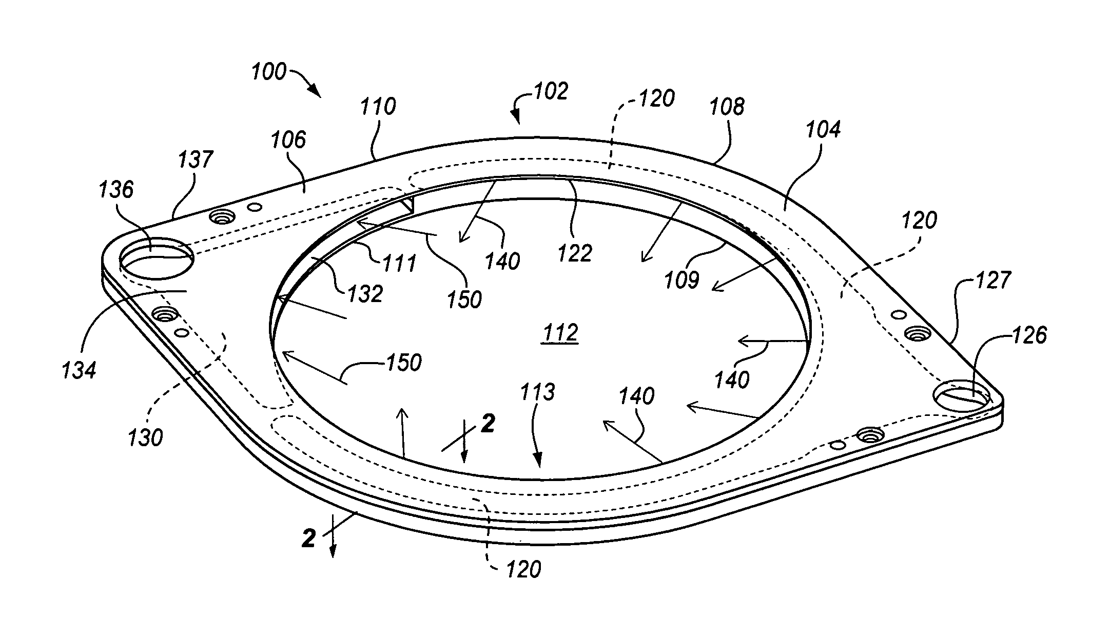
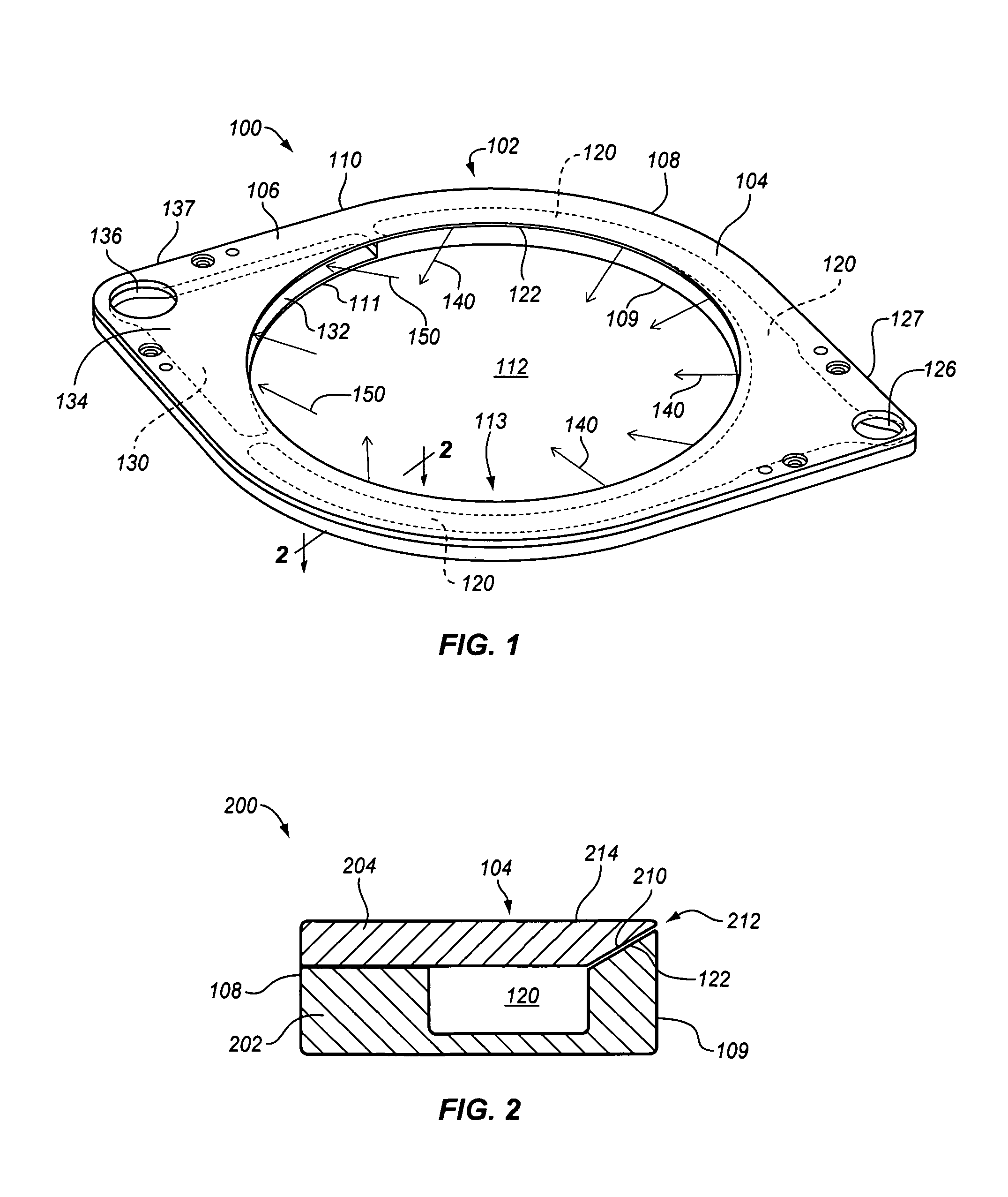
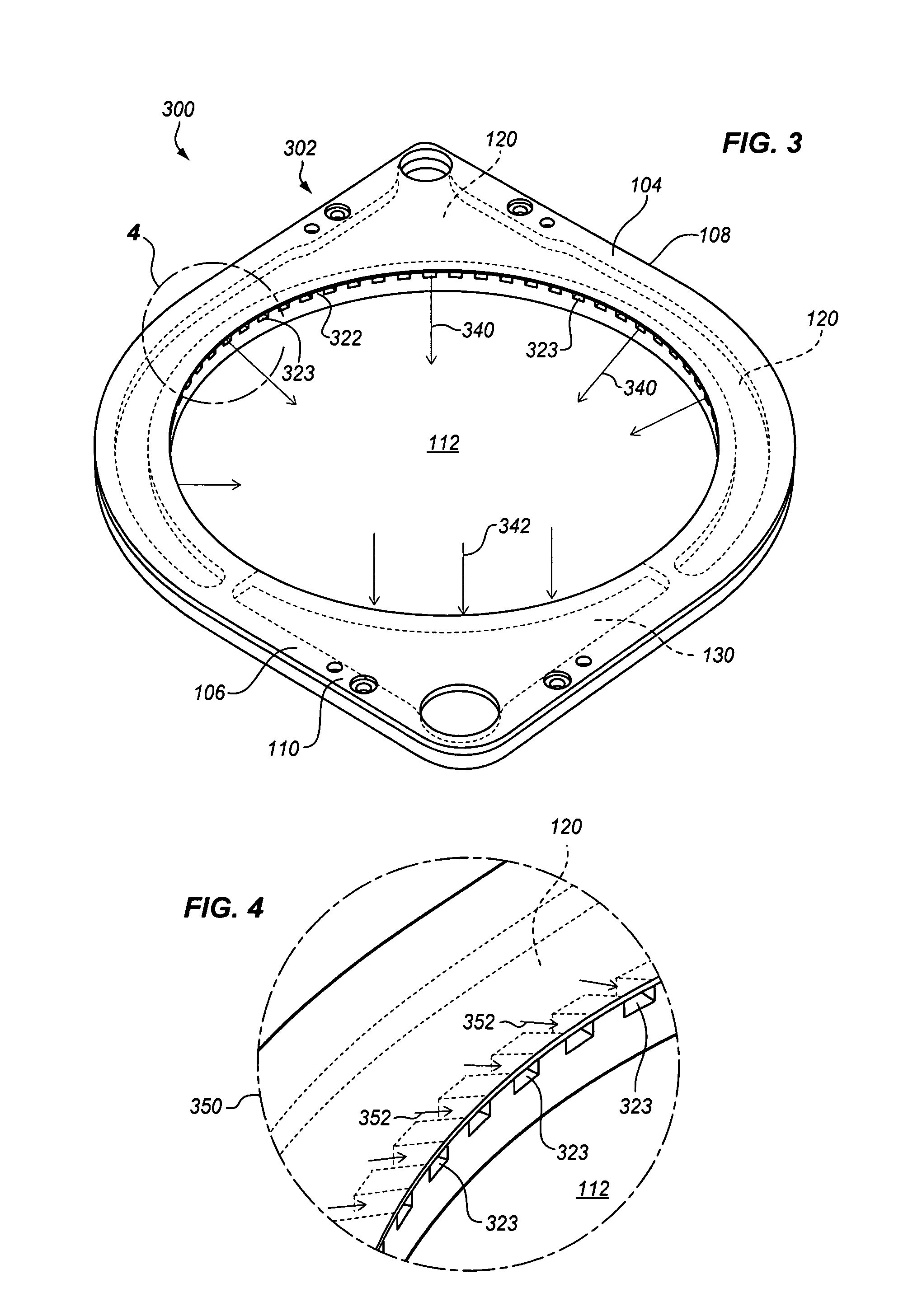
[0044]FIG. 5 depicts a perspective view 400 of lower part 402 of a purge ring in accordance with the invention before assembly with an upper part. FIG. 6 depicts a perspective view 404 of an upper part 406 for assembling together with a lower part 402 (FIG. 5) to make a purge ring in accordance with the invention. As depicted in FIG. 5, lower part 402 comprises an inlet portion 410. Inlet portion 410 includes a recessed region 412 that serves to form an inlet plenum in a purge ring when lower part 402 is assembled together with a corresponding upper part 406. Lower part 402 further includes an exhaust portion 420. Exhaust portion 420 includes a recessed region 422 that serves to form an exhaust channel in a purge ring when lower part 402 is assembled together with a corresponding upper part 406. As depicted in FIG. 6, upper part 406 includes an inlet portion 440 and an exhaust portion 450 that mate together with inlet portion 410 and exhaust portion 420, respectively, of lower part ...

example 2

[0066]A ULK thin film having a thickness of about 300 nm and containing porogens was formed on each of a series of 300 mm wafers. The ULK thin films were cured in a four-station curing chamber, as depicted in FIG. 9. During curing, purging of the curing stations was conducted in accordance with the invention. One thousand wafers were processed consecutively, whereby an intermittent cleaning of the apparatus was conducted after each group of 75 wafers. Then, physical properties of the dielectric films were measured.

[0067]Curing was conducted in a model SOLA ultraviolet thermal processing (UVTP) tool comprising a multistation sequential curing chamber, commercially available from Novellus Systems, Inc. The curing tool included four curing station units and a MKS HF-s Astron remote plasma cleaning unit contained within the curing chamber. A purge ring having specifications as described in Example 1 was mounted as depicted schematically in FIG. 7 at each of purge Stations 1-4. At Statio...

example 3

[0070]Under conditions similar to those described with reference to Example 2 above, approximately 120 wafers containing a deposited film of dielectric material were cured with purging in accordance with the invention without intermittent cleaning.

[0071]After curing, the density of each of the cured dielectric films was measured by measuring film shrinkage. Film shrinkage was determined by measuring film thickness using a model Optiprobe device commercially available from Thermawave, then comparing post-curing thickness to pre-curing thickness. With the density of the dielectric film on the first cured wafer as a standard of comparison, the relative density of each of the subsequently cured films was calculated. The relative density is referred to as the relative curing effectiveness since it indicates the ability of a curing system with purging in accordance with the invention to remove porogens from successively cured dielectric films. FIG. 11 contains a graph in which relative cu...


PUM

PropertyMeasurementUnit
Lengthaaaaaaaaaa
Angleaaaaaaaaaa
Angleaaaaaaaaaa

Abstract

An apparatus for purging a space in a processing chamber comprises a source of a purge gas; an inlet portion of a purge ring; an inlet baffle located in the inlet portion and fluidically connected to the source of purge gas; and an exhaust portion of the purge ring. The inlet portion and the exhaust portion define a ring hole space having a 360° periphery. The inlet baffle preferably surrounds not less than 180° of said periphery. The inlet baffle is operable to convey purge gas into the ring hole space. The exhaust portion is operable to convey purge gas and other matter out of the ring hole space. Cleaning of the purge ring and other structures in a processing chamber is conducted by flowing a cleaning gas through the inlet baffle. Methods and systems using a purge ring are particularly useful for purging and cleaning porogens from a UV curing chamber. Some embodiments include a gas inlet plenum and an exhaust channel but not a purge ring.

Description

RELATED APPLICATIONS[0001]This application is a divisional application, claiming priority under 35 USC §§120 and 121 and 37 CFR 1.53(b) of co-owned U.S. patent application Ser. No. 11 / 391,134, filed Mar. 28, 2006, by Smargiassi et al., now abandoned, which claims the benefit under 35 USC 119(e) of U.S. Provisional Application Ser. No. 60 / 742,844, filed Dec. 5, 2005. This application is also a continuation-in-part application, claiming priority under 35 USC 120, of co-owned U.S. patent application Ser. No. 11 / 115,576 filed Apr. 26, 2005, now U.S. Pat. No. 8,137,465 having the title “Single Chamber Sequential Curing of Semiconductor Wafers”. These parent applications are incorporated herein by reference for all purposes.FIELD OF THE INVENTION[0002]The invention is related to the field of integrated circuit fabrication, in particular to methods and apparatuses for purging and cleaning process chambers used in the annealing and curing of semiconductor wafers.BACKGROUND OF THE INVENTION[...

Claims


Application Information

Patent Timeline
IPC IPC(8): C23F1/00H01L21/306
CPCH01L21/02041H01L21/67017H01L21/02203H01L21/02348H01L21/67115H01L21/6719H01L21/67207
Inventor SMARGIASSI, EUGENELAU, STEPHEN YU-HONGKAMIAN, GEORGE D.XI, MING
Owner NOVELLUS SYSTEMS
Why Eureka
Try Eureka