Display device

a technology of display device and display screen, which is applied in the field of display device, can solve the problems of different writing time of video signal different ratio of the returned level of com voltage to the original level of com voltage for each group of pixels, and high brightness

Inactive Publication Date: 2009-09-24
JAPAN DISPLAY WEST
View PDF5 Cites 0 Cited by
  • Summary
  • Abstract
  • Description
  • Claims
  • Application Information

AI Technical Summary

Benefits of technology

[0019]An electronic device according to a second aspect of the invention includes the display device according to the first aspect of the invention. By providing such a configuration,...

Problems solved by technology

Therefore, the pulse width of each of the two kinds of sampling pulses becomes unequal, and thus, the inequality causes a difference between durations while respective groups of the switch sections, corresponding to the two kinds of the sampling pulses, are under the turned-on condition, and further, the difference leads to a disadvantage in which the writing time of video signals is different for each group of pixels which corresponds to one of the two groups of the switch sections.
Furthermore, when, upon receipt of a sampling pulse, the switch sections connected to the data lines turn on, the level of a COM voltage is likely to vary due to parasitic capacitance being generated between the data lines and ...

Method used


Image

  • Display device
  • Display device
  • Display device

Examples


first embodiment

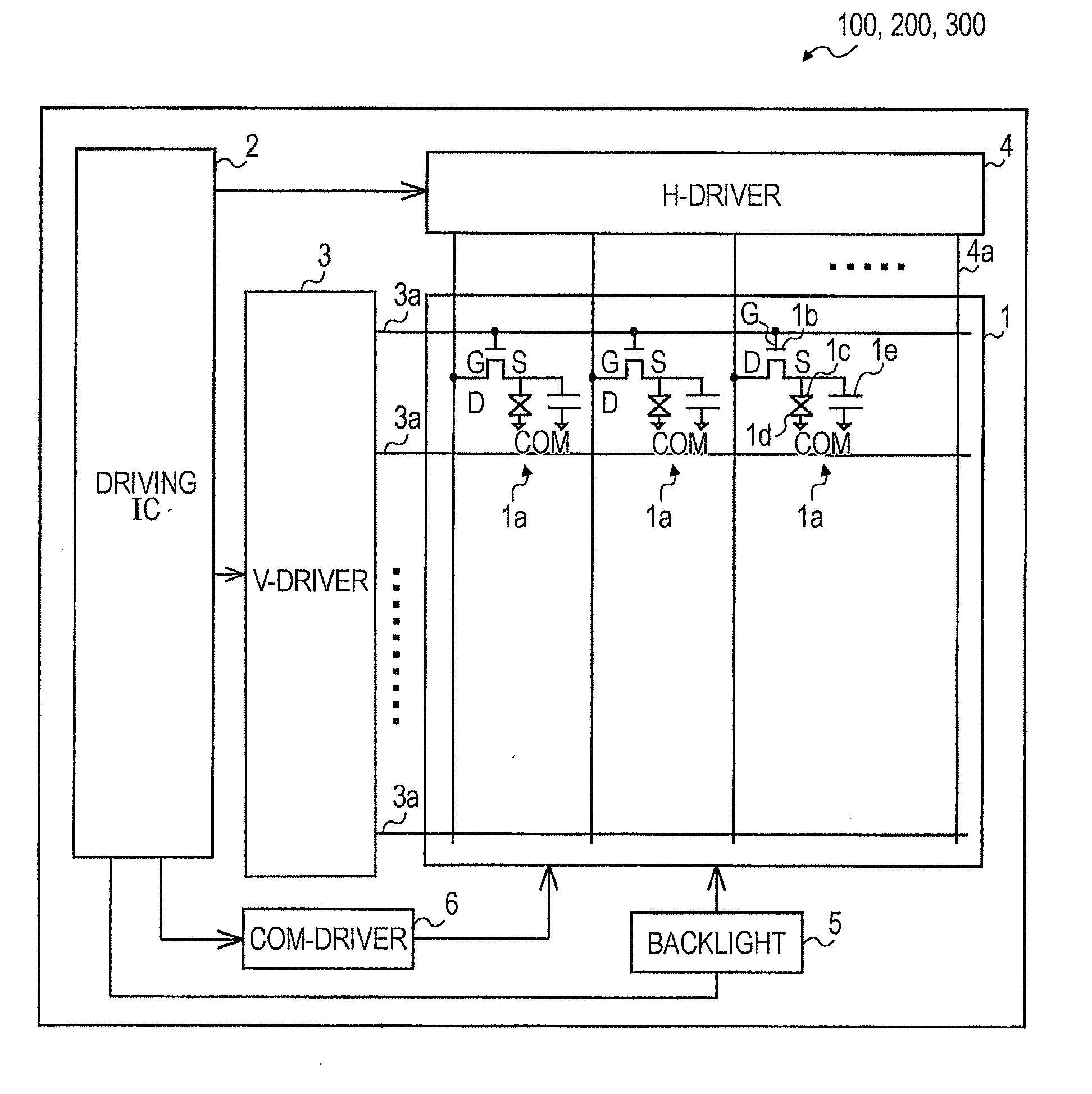
[0035]FIG. 1 is a block diagram depicting an overall configuration of a liquid crystal display device according to a first embodiment of the invention. FIGS. 2 to 4 are diagrams, each being used for describing a detailed configuration of the liquid crystal display device according to the first embodiment of the invention. Firstly, a configuration of a liquid crystal display device 100 according to the first embodiment of the invention will be described with reference to FIGS. 1 to 4. In addition, in the first embodiment of the invention, the liquid crystal display device will be described as an example of the display devices to which the invention is applied.

[0036]As shown in FIG. 1, the liquid crystal display device 100 includes a display screen section 1, a driving IC 2, a V-driver 3, an H-driver 4, a backlight 5, and a COM-driver 6. In the display screen section 1, a plurality of pixels 1a are arranged in a matrix. In addition, in FIG. 1, only three pixels 1a are shown for the sa...

second embodiment

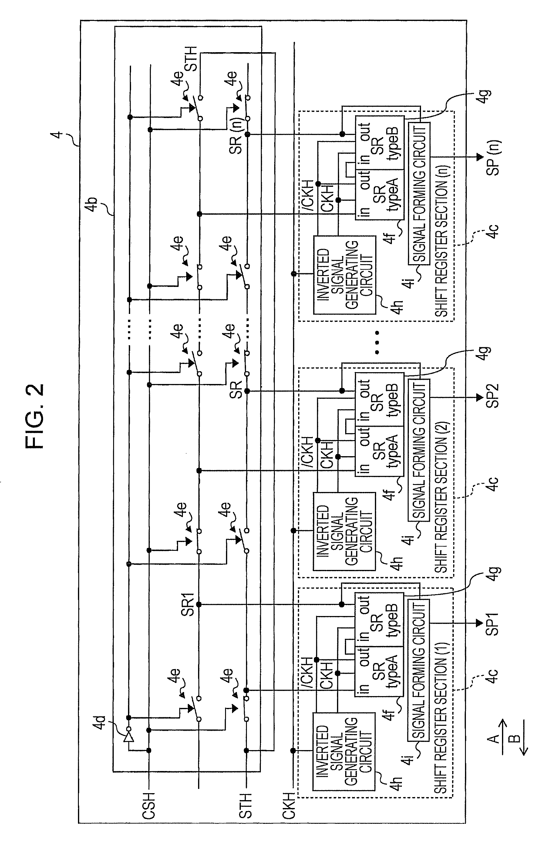
[0067]FIGS. 10 and 11 are diagrams each depicting a configuration of a liquid crystal display device according to a second embodiment of the invention. In the second embodiment of the invention, differing from the first embodiment in which each of the shift register sections 4c is configured to be supplied with an one-phase clock signal, a liquid crystal display device 200 in which each of the shift register sections 4c is configured to be supplied with two-phase clock signals having mutually inverted phases will be described.

[0068]As shown in FIG. 10, the liquid crystal display device 200 according to the second embodiment of the invention is configured to supply two clock signals having mutually inverted phases (i.e., a CKH signal and a / CKH signal) to the shift register 4f and the shift register 4g in each of the shift register sections 4c. In addition, configurations other than this configuration in the second embodiment are the same as those in the first embodiment of the inven...

third embodiment

[0071]FIG. 12 is a timing chart depicting operations in the third embodiment of the invention. In the third embodiment of the invention, operations in the case where the pulse width of the STH signal (i.e., the start signal) is wider than that in the above-described first embodiment will be described with reference to FIG. 12. Additionally, the configuration of the liquid crystal display device 300 according to the third embodiment of the invention is the same as that of the liquid crystal display device 100 according to the first embodiment of the invention.

[0072]In the third embodiment of the invention, the pulse width of the start signal, which is configured to be substantially equal to one clock period of the clock signal in the operations associated with the first embodiment of the invention shown in FIG. 5 (i.e., operations in a non-overlapping method in which, subsequent to completion of the writing of the video signals into a certain pixel block, the writing into a next pixe...


PUM


Abstract

A display device includes a plurality of shift register sections, each being configured to sequentially generate a sampling pulse for writing a video signal into a pixel, wherein each of the plurality of shift register sections includes an even number of shift registers, and wherein one sampling pulse is generated by each of the plurality of shift register sections, and substantially all of the sampling pulses are generated on the basis of either the rising edges of a clock signal or the falling edges of a clock signal, whichever is selected in advance.

Description

BACKGROUND[0001]1. Technical Field[0002]The present invention relates to display devices and, more particularly, to a display device including a plurality of shift registers.[0003]2. Related Art[0004]To date, display devices including a plurality of shift registers have been well known to those skilled in the art (refer to, for example, JP-A-2003-122322).[0005]In JP-A-2003-122322 described above, a liquid crystal display apparatus including switch sections (HSW) located between data lines and image signal lines, and further, shift registers configured to generate control signals (i.e., sampling pulses) for performing control of turning on / off of the switch sections has been disclosed. The liquid crystal display device disclosed in JP-A-2003-122322 described above is configured to generate the sampling pulses on the basis of the rising edges and falling edges of a clock signal and sequentially output the sampling pulses to the switch sections.[0006]However, the liquid crystal display...

Claims


Application Information

Patent Timeline
IPC IPC(8): G09G3/20
CPCG09G3/3688G09G2320/0209G09G2310/0286G02F1/133G09G3/36
Inventor MATSUURA, YOSHIYUKI
Owner JAPAN DISPLAY WEST
Why Eureka
Try Eureka