Display device

a display device and photosensor technology, applied in the field of display devices, can solve the problems of increasing manufacturing costs, increasing manufacturing costs, and increasing manufacturing costs

Active Publication Date: 2009-09-24
JAPAN DISPLAY WEST
View PDF3 Cites 14 Cited by
  • Summary
  • Abstract
  • Description
  • Claims
  • Application Information

AI Technical Summary

Benefits of technology

[0007]An advantage of some aspects of the invention is that it provides a display device that includes a light amount detecting device that has a sensitivity correction function and may be manufactured in a simple process.

Problems solved by technology

However, the photoelectric conversion element described in JP-A-9-232620 requires a special manufacturing condition, so manufacturing cost problematically increases.
Specifically, when a photosensor is provided inside a display device that uses a thin film transistor or when a display device and a photosensor are manufactured by the same equipment, it is impossible to manufacture the photosensor together with a driving transistor of the display device.
This causes an increase in manufacturing cost and, in addition, increases power consumption.

Method used


Image

  • Display device
  • Display device
  • Display device

Examples


first embodiment

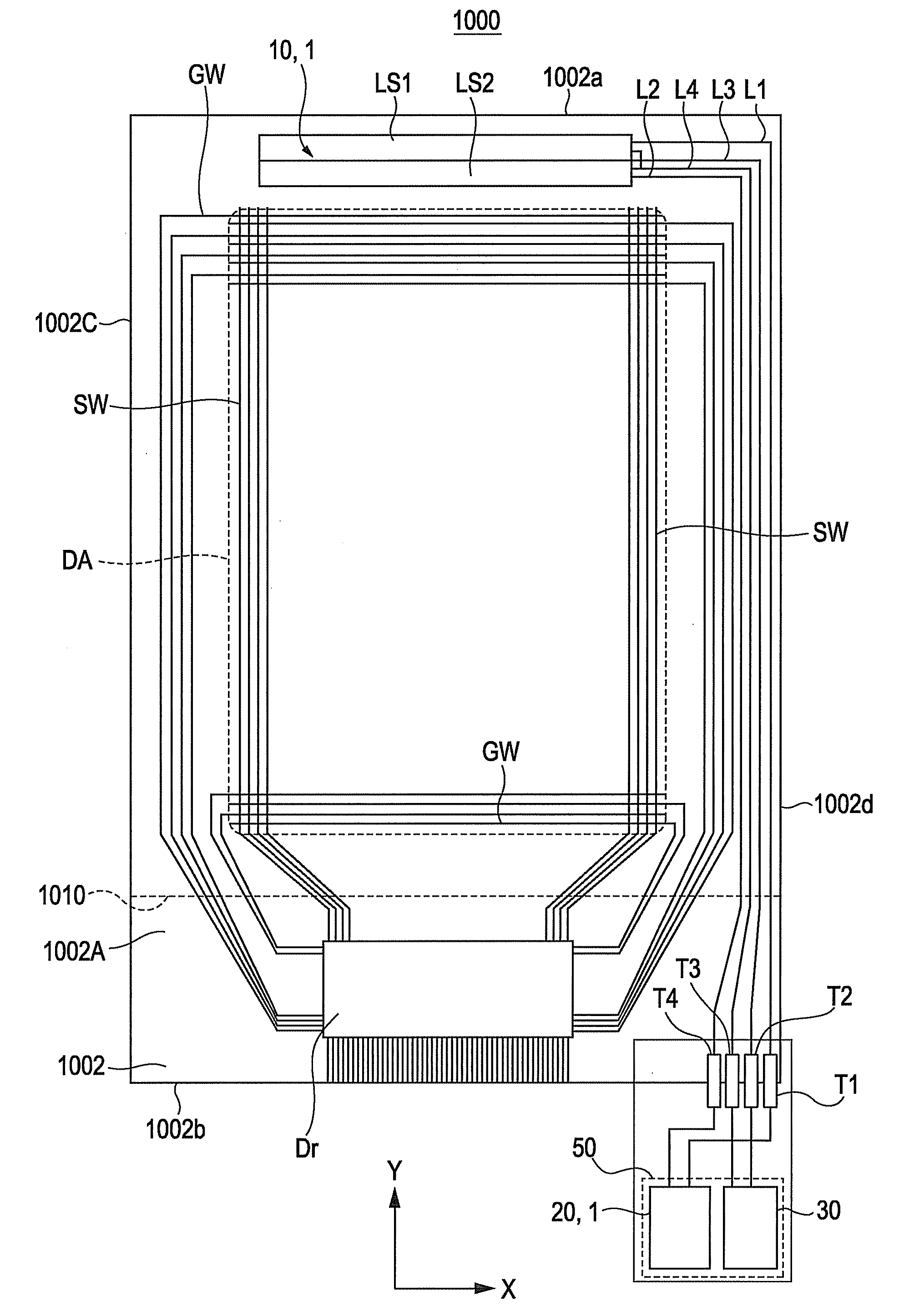
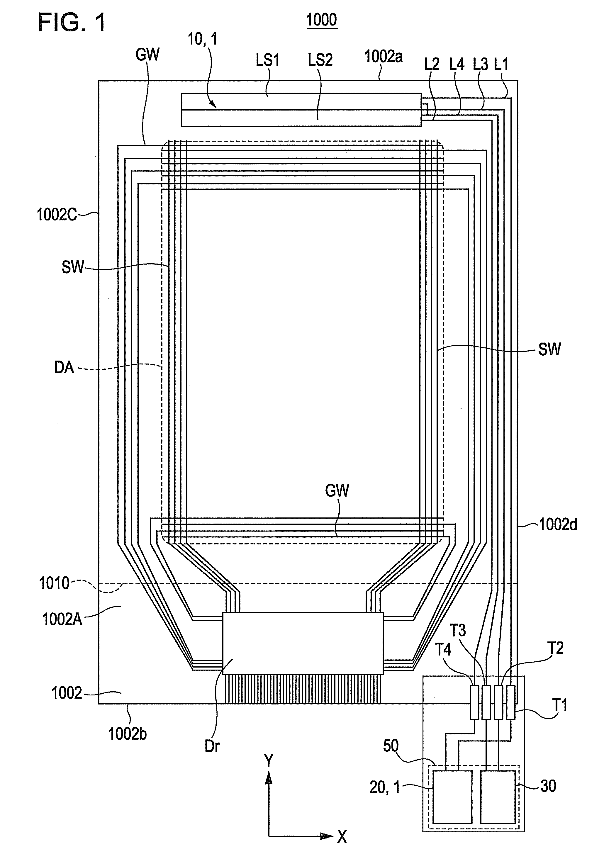
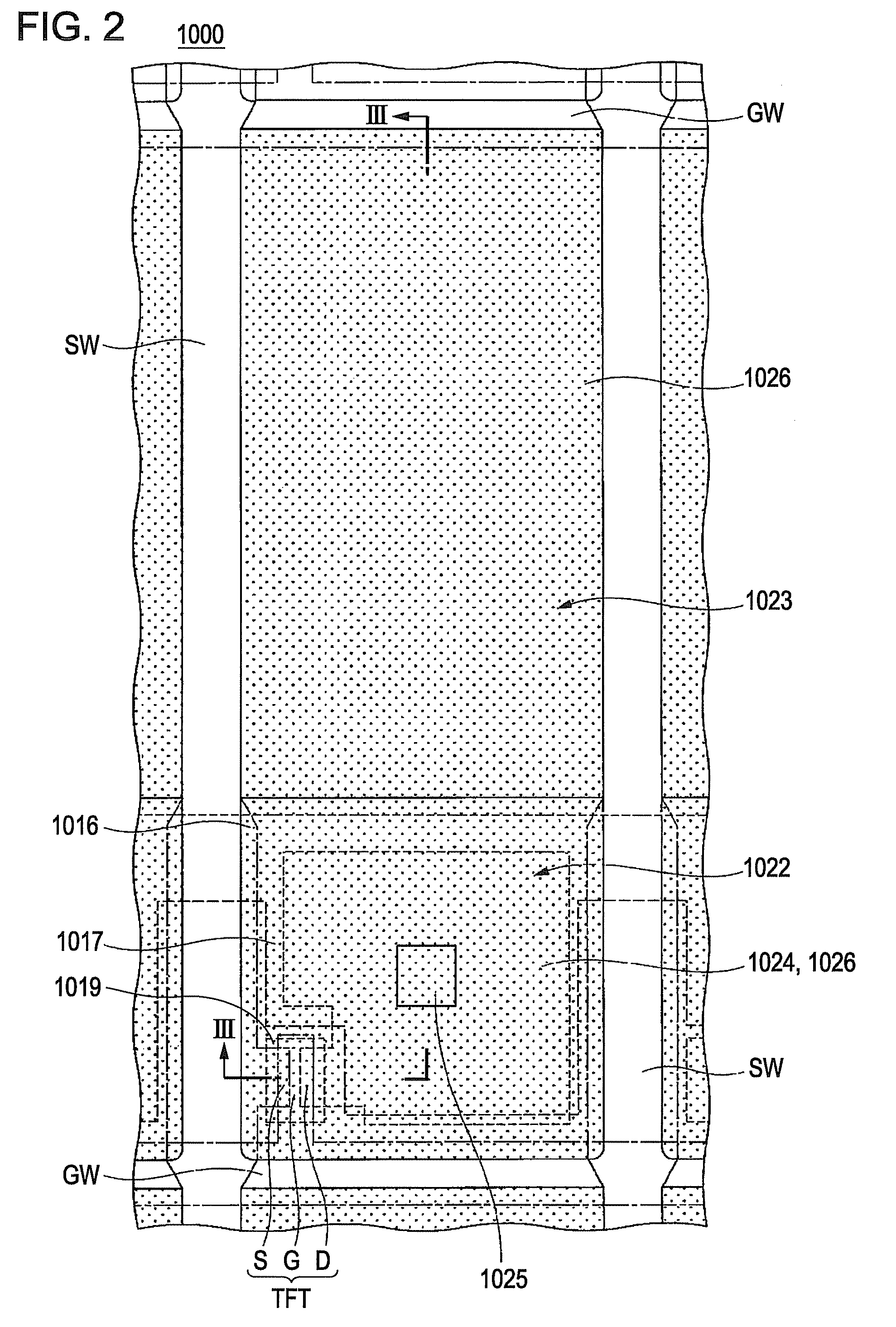
[0040]FIG. 1 is a schematic plan view of an array substrate in a transflective liquid crystal display device (display device / electro-optical device) according to a first embodiment of the invention. Note that FIG. 1 is shown as viewed through a color filter substrate. FIG. 2 is a plan view of one pixel on the array substrate shown in FIG. 1. FIG. 3 is a cross-sectional view that is taken along the line III-III in FIG. 2.

[0041]As shown in FIG. 1, the liquid crystal display device 1000 includes the array substrate AR and the color filter substrate CF, which are arranged so as to face each other. The array substrate AR is formed so that various wires, and the like, are formed on a transparent substrate 1002 made of a rectangular transparent insulating material, such as glass plate. The color filter substrate CF is formed so that various wires, and the like, are formed on a transparent substrate 1010 made of a similar rectangular transparent insulating material. The array substrate AR h...

second embodiment

[0108]Next, a second embodiment will be described. In the second embodiment, potential signals output from the photodetection unit 10 to the photosensor reader unit 20 are read as photoelectric currents, and the photoelectric currents are logarithmically transformed and then calculated.

[0109]First, a calculation method through logarithmical transformation will be described. When the photodegradation power correction coefficient K in the first embodiment is logarithmically transformed, Log2K=Log2{(Ia′(L1) / Ib′(L1 / n)) / (Ia(L0) / Ib(L0 / n))}=(Log2(Ia′(L1))−Log2(Ib′(L1 / n)))−(Log2(Ia(L0))−Log2(Ib(L0 / n))). Then, when the photodegradation slope correction coefficient K″ is logarithmically transformed, Log2K″=Log2(Ia″(L1) / Ib″(L1)) / (Ia(L1) / Ib(L1))=Log2(Ia″(L1))−Log2(Ib″(L1))−(Log2(Ia(L1))−Log2(Ib(L1))). Thus, through logarithmical transformation, multiplication and division are replaced with addition and subtraction.

[0110]By so doing, from the logarithmically transformed power correction coeffici...


PUM


Abstract

A display device includes: first and second photosensors; a reader; a light detector outputting the light amount detected by the photosensors; a first circuit outputting a first signal based on incident light entering the first photosensor; and a second circuit outputting a second signal based on dimmed incident light entering the second photosensor. The reader includes: a coefficient calculator calculating a first measurement ratio of the first signal to the second signal, and a power correction coefficient; a rate calculator deriving modified power coefficients from the power correction coefficient, calculating a second measurement ratio of the power-corrected first and second signals, and calculating a slope correction coefficient; and an output unit deriving modified proportional coefficients from the slope correction coefficient, and correcting the power-corrected first and second signals using the modified proportional coefficients to yield outputted initial light amount signals.

Description

BACKGROUND[0001]1. Technical Field[0002]The invention relates to a display device and, more particularly, to a display device that includes a light amount detecting device having a sensitivity correction function in consideration of degradation of a photosensor and may be manufactured in a simple process.[0003]2. Related Art[0004]An known existing light amount detection circuit utilizes the relationship that a leakage current from a thin film transistor is proportional to the amount of light received, makes a voltage detecting capacitor charge or discharge electric charge by the leakage current, and then monitors a voltage variation between both ends of the capacitor to thereby detect the amount of light (for example, see JP-A-2006-29832). Incidentally, it is generally known that the leakage current from the thin film transistor is proportional to the amount of light received; however, the sensitivity, which is a leakage current value against the amount of light received, decreases ...

Claims


Application Information

Patent Timeline
Patent Type & Authority Applications(United States)
IPC IPC(8): G09G5/00
CPCG09G3/3611G09G2360/144G09G2320/0626G09G3/3648
Inventor KUNIMORI, TAKASHI
Owner JAPAN DISPLAY WEST
Why Eureka
Try Eureka