Solid-state image pickup apparatus

a pickup apparatus and solid-state technology, applied in the field of solid-state image pickup apparatus, can solve the problems of difficult to make the length of the gate electrode of the transistor, difficult to make the area of the gate electrode that is oriented to each other after processing, and complicated driving-related timing, etc., to reduce the difference in dark current.

Inactive Publication Date: 2009-09-24
CANON KK
View PDF10 Cites 35 Cited by
  • Summary
  • Abstract
  • Description
  • Claims
  • Application Information

AI Technical Summary

Benefits of technology

[0005]The present invention, according to aspects thereof, provides a technique for reducing the difference in dark current between photoelectric ...

Problems solved by technology

However, in adjacent pixels, it is very difficult to make the lengths of gate electrodes of transistors and the potentials of these gate electrodes during an accumulation period conform to each other.
Accordingly, it is more difficult to make the areas of these gate electrodes conform to each other after processing.
If the number of transistors for shared use increases, driving-related timing becomes complicated.
It is therefore difficult to make the potentials of these gate electrodes conform to each other during the accumulat...

Method used


Image

  • Solid-state image pickup apparatus
  • Solid-state image pickup apparatus
  • Solid-state image pickup apparatus

Examples


first embodiment

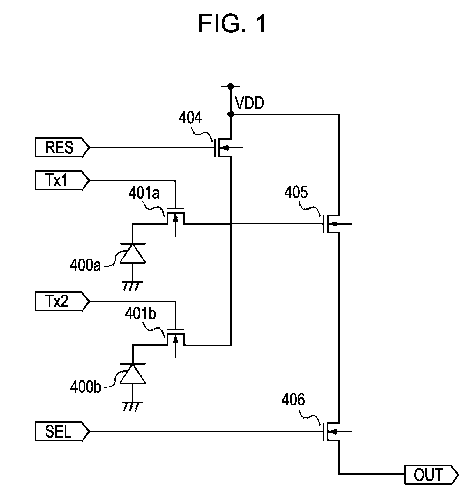
[0028]FIG. 1 is a diagram illustrating an equivalent circuit of a solid-state image pickup apparatus according to a first embodiment. The solid-state image pickup apparatus includes a first photoelectric conversion element 400a and a second photoelectric conversion element 400b, which are photodiodes in this embodiment. In this drawing, only two photoelectric conversion elements are illustrated. However, a larger number of photoelectric conversion elements may be included in a solid-state image pickup apparatus according to this embodiment.

[0029]Transfer portions 401a and 401b for transferring the electric charge of a photoelectric conversion element are MOS transistors in this embodiment. A reset portion 404, for resetting the input portion of an amplification portion to be described later by setting the potential of a gate electrode of the amplification portion to a reference potential, is a MOS transistor in this embodiment. An amplification portion 405 for amplifying a signal co...

second embodiment

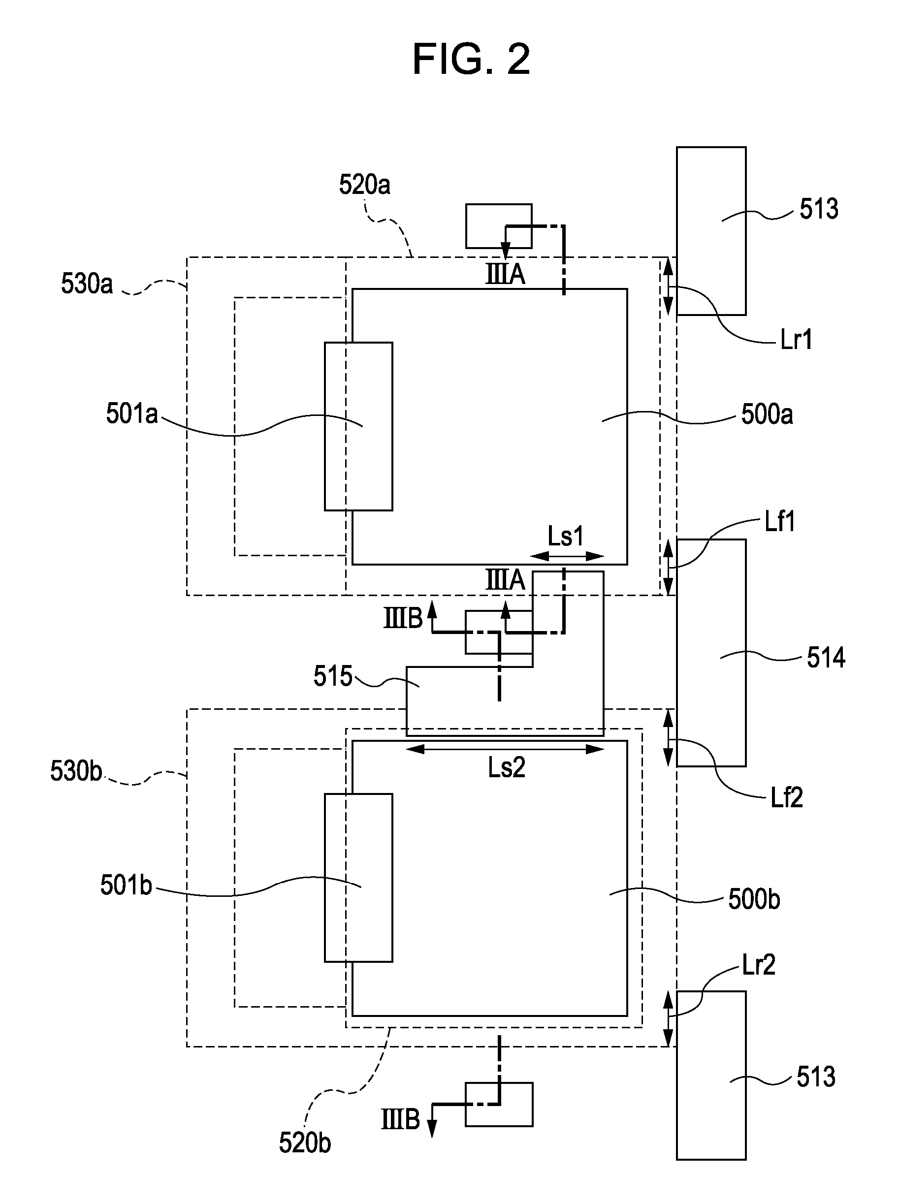
[0056]FIG. 4 is a plan view of a solid-state image pickup apparatus according to a second embodiment. FIG. 5A is a cross-sectional view taken along the line VA of FIG. 4, and FIG. 5B is a cross-sectional view taken along the line VB of FIG. 4. The same reference numerals are used to identify parts already described in the first embodiment, and the descriptions thereof will be therefore omitted. In this embodiment, the areas of antireflection coating films are the same, but the areas (widths) of channel stop regions are made to differ from each other. In this embodiment, the area of a channel stop region denotes an area in the top view of the channel stop region.

[0057]Like in the first embodiment, in this embodiment, the lengths of portions of respective gate electrodes of MOS transistors that face respective adjacent photoelectric conversion elements are different from each other. Referring to FIG. 4, the length of a portion of a gate electrode of each MOS transistor facing the firs...

third embodiment

[0060]FIG. 6 is a plan view of a solid-state image pickup apparatus according to a third embodiment. FIG. 7A is a cross-sectional view taken along the line VIIA of FIG. 6, and FIG. 7B is a cross-sectional view taken along the line VIIB of FIG. 6. The same reference numerals are used to identify parts already described in the first and second embodiments, and the descriptions thereof will be therefore omitted.

[0061]In this embodiment, a case in which a period during which a voltage lower than that in the first and second embodiments (non-conducting voltage) is applied to a gate electrode is long in the accumulation period of a photoelectric conversion element will be described. For example, during the whole accumulation period of each photoelectric conversion element, a voltage for bringing a MOS transistor out of conduction is applied to the gate electrodes of a plurality of MOS transistors. These MOS transistors are disposed for each photoelectric conversion element, and include a ...


PUM


Abstract

A solid-state image pickup apparatus includes a first antireflection coating film formed on a light-receiving surface of a first photoelectric conversion element and a second antireflection coating film formed on a light-receiving surface of a second photoelectric conversion element. A total length of first photoelectric conversion element facing portions of gate lines adjacent to the first photoelectric conversion element is shorter than a total length of second photoelectric conversion element facing portions of gate lines adjacent to the second photoelectric conversion element. An area of the first antireflection coating film is larger than that of the second antireflection coating film.

Description

FIELD OF THE INVENTION[0001]The present invention relates to a solid-state image pickup apparatus used for a digital camera, a digital video camera, a copier, or a facsimile machine, and also relates to a camera using the solid-state image pickup apparatus.BACKGROUND OF THE INVENTIONDescription of the Related Art[0002]An increasing number of pixels are included in solid-state image pickup apparatuses. In amplifying-type solid-state image pickup apparatuses, which include pixels each including an amplifying MOS transistor, in order to increase the number of pixels in a limited chip area, a pixel reading circuit is shared among a plurality of photoelectric conversion elements. Methods of decreasing the number of transistors for a single photoelectric conversion element are therefore used.[0003]A method of reducing the difference in dark current between pixels connected to each other is disclosed in Japanese Patent Laid-Open No. 2006-074009. Using this method, the difference in dark cu...

Claims


Application Information

Patent Timeline
IPC IPC(8): H04N5/335H01L27/146
CPCH01L27/14603H01L27/14641H04N5/37457H01L27/1463H04N25/778
Inventor HATANO, YUUICHIROUTAKADA, HIDEAKIHIYAMA, HIROKI
Owner CANON KK
Why Eureka
Try Eureka