Enhanced Thermal Dissipation Ball Grid Array Package

a grid array and thermal dissipation technology, applied in the field of semiconductor packaging, can solve the problems of less reliable mold compounds, greater challenges, damage to chips, etc., and achieve the effect of low thermal conductivity

Active Publication Date: 2009-10-01
SYNAPTICS INC
View PDF13 Cites 23 Cited by
  • Summary
  • Abstract
  • Description
  • Claims
  • Application Information

AI Technical Summary

Problems solved by technology

In the extreme, if a semiconductor chip is allowed to get too hot it can damage the chip.
As chips become higher performance, they pose a greater challenge as they consume more power and generate more heat.
However, in addition to the expense, these mold compounds are less reliable, and are more difficult to use in the transfer molding operation.
However, these configurations are much more expensive in fact they are two to five times more expensive to manufacture.

Method used


Image

  • Enhanced Thermal Dissipation Ball Grid Array Package
  • Enhanced Thermal Dissipation Ball Grid Array Package
  • Enhanced Thermal Dissipation Ball Grid Array Package

Examples


Embodiment Construction

[0019]A detailed description of embodiments of the present invention is presented below. While the disclosure will be described in connection with these drawings, there is no intent to limit it to the embodiment or embodiments disclosed herein. On the contrary, the intent is to cover all alternatives, modifications and equivalents included within the spirit and scope of the disclosure as defined by the appended claims.

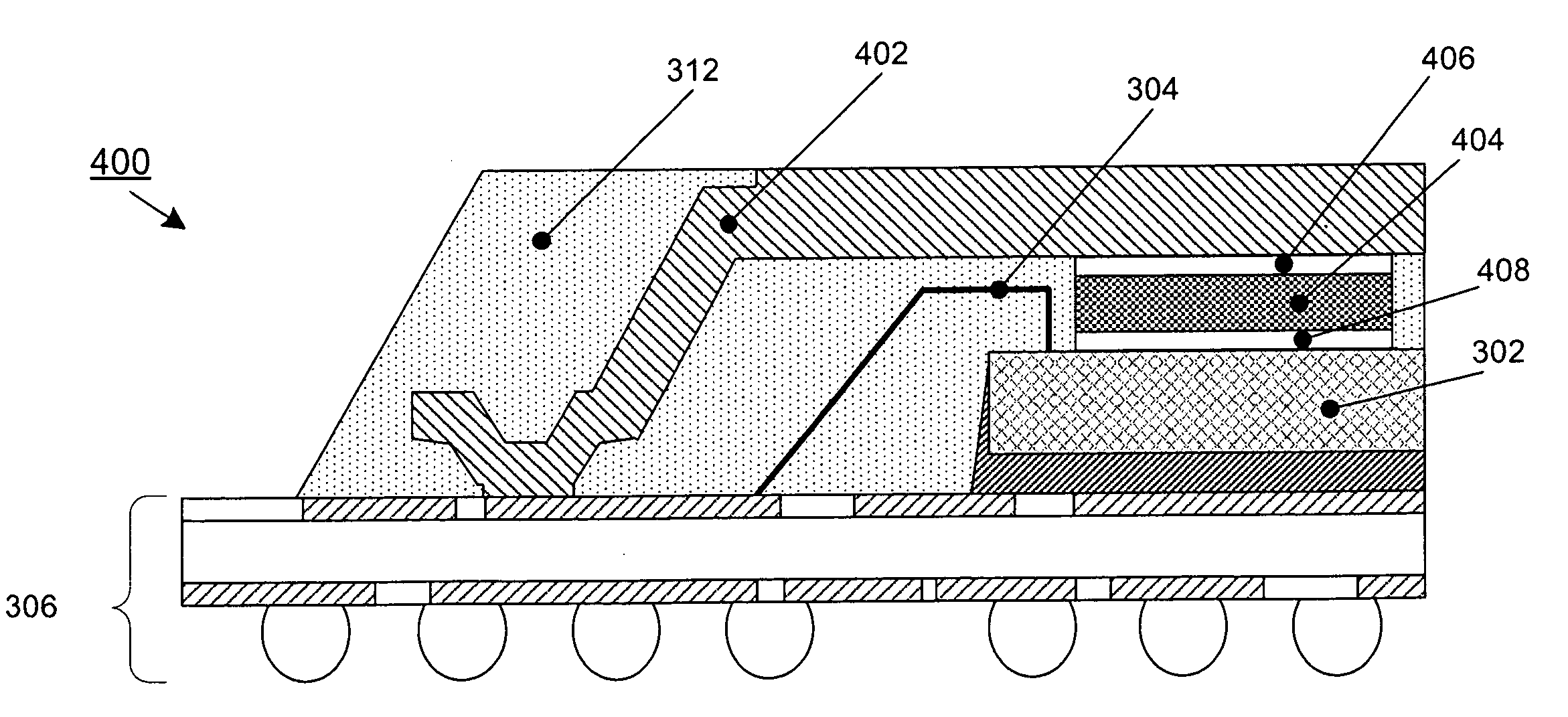
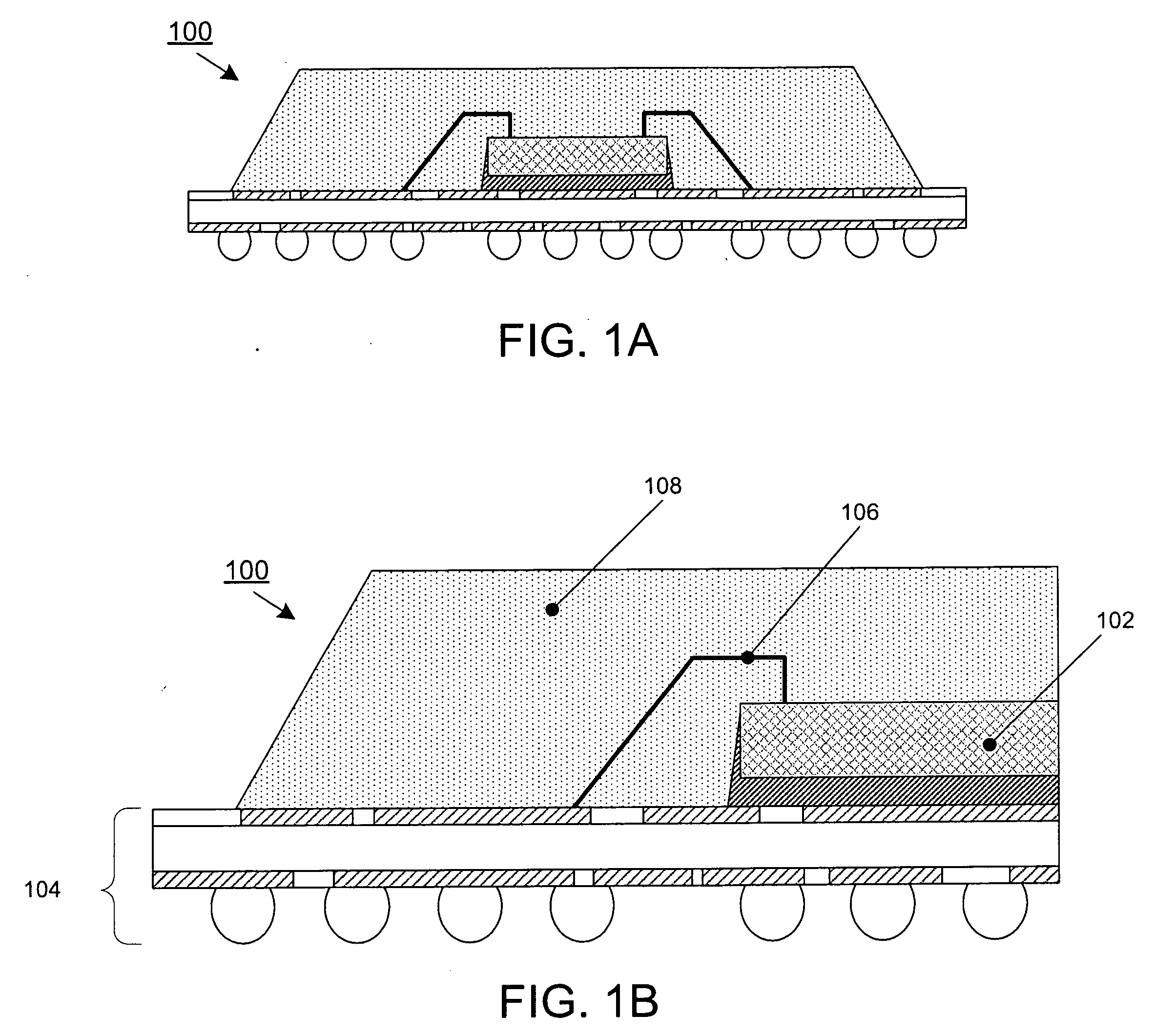
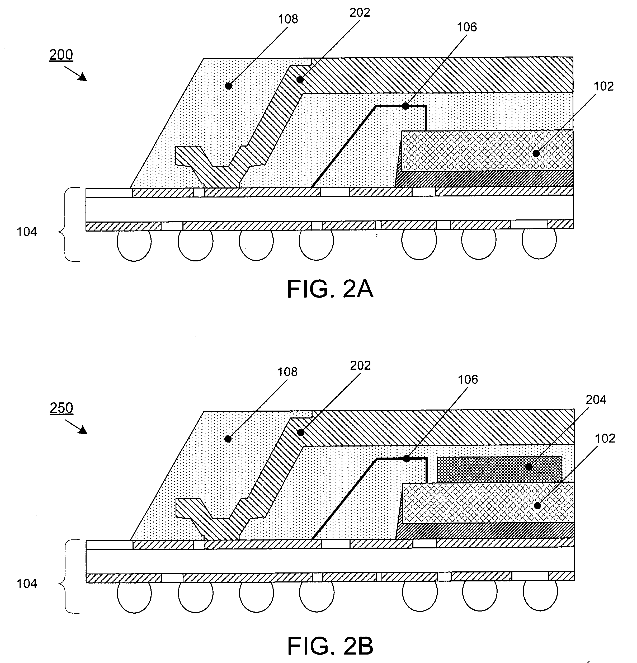
[0020]FIG. 3 illustrates the first embodiment. As in the prior art, semiconductor chip package 300 comprises functional die 302, wire bond 304 and interface 306. Chip package 300 further comprises internal heat spreader 308. However, thermal adhesive 310 is applied to functional die 302 and bonds to heat spreader 308. This places a direct thermal conductivity path from the functional die to the heat spreader without package material between the functional die and heat spreader. Heat spreader 308 typically comprises a metal which is often copper.

[0021]Thermal adhesive 3...


PUM


Abstract

In a semiconductor chip, a thermal adhesive is used to bond an internal heat spreader to an active functional die. In an alternative embodiment a dummy die is place directly on top of the active functional die and a thermal adhesive is used to bond an internal heat spreader to the dummy die. This provides a direct and relatively low thermal conductivity path from the heat source, i.e., the functional device to the top of the package, that is, the internal metal heat spreader which is also exposed to the air.

Description

BACKGROUND OF THE INVENTION[0001]1. Field of the Inventions[0002]The invention relates generally to semiconductor packaging and specifically to improving heat dissipation within a semiconductor chip.[0003]2. Background Information[0004]Heat dissipation is essential in semiconductor chips. In the extreme, if a semiconductor chip is allowed to get too hot it can damage the chip. Even outside of this extreme semiconductor chips are designed to operate within a particular temperature range. In order to maintain a chip within its operating temperature range, heat must be drawn away from the chip. As chips become higher performance, they pose a greater challenge as they consume more power and generate more heat.[0005]FIG. 1A illustrates a basic semiconductor chip package in cross-section. FIG. 1B is a close up view of semiconductor chip package 100. It should be noted that all figures in this disclosure are conceptual representations and components contained in these diagrams are not nece...

Claims


Application Information

Patent Timeline
Patent Type & Authority Applications(United States)
IPC IPC(8): H01L23/34H01L21/50H01L21/56
CPCH01L23/4334H01L2224/48227H01L2924/16152H01L24/48H01L2924/10253H01L2924/01019H01L2924/00H01L2924/00014H01L2924/14H01L2924/181H01L2924/00012H01L2224/45099H01L2224/45015H01L2924/207
Inventor WARREN, ROBERT W.
Owner SYNAPTICS INC
Why Eureka
Try Eureka