Microwave Cure of Semiconductor Devices

a technology of semiconductor devices and curing methods, which is applied in the manufacture of microstructural devices, semiconductor devices, electrical devices, etc., can solve the problems of many problems in the curing process, the device is damaged, and the entire structure is heated, so as to reduce the number of defects, reduce stress, and reduce the effect of curing speed

Inactive Publication Date: 2009-10-08
TEXAS INSTR INC
View PDF7 Cites 6 Cited by
  • Summary
  • Abstract
  • Description
  • Claims
  • Application Information

AI Technical Summary

Benefits of technology

[0011]An advantage of a preferred embodiment of the present invention is the reduced number of defects by only selectively heating the adhesive or encapsulant, thereby reducing the stresses normally caused by differing coefficients of thermal expansion.
[0012]A further advantage of a preferred embodiment of the present invention is that microwave curing is much quicker than thermal curing of the adhesive or encapsulant. This allows for much better overall process control and debottlenecking opportunities.

Problems solved by technology

However, this thermal curing process has many problems associated with it.
One of the larger problems is that by using convective heat transfer, the entire structure, and not just the material that is desired to be cured, is heated.
These stresses may cause defects in the device, shifts in the alignment of the materials, and reduce overall yields to an unacceptable level.
Further, thermal curing is a time consuming process.
Such a length of time is not only lengthy in and of itself, but may easily become a bottleneck to the overall manufacturing process.
Such a movement could easily cause the individual pieces to become mis-aligned.

Method used


Image

  • Microwave Cure of Semiconductor Devices
  • Microwave Cure of Semiconductor Devices
  • Microwave Cure of Semiconductor Devices

Examples


Embodiment Construction

[0021]The making and using of the presently preferred embodiments are discussed in detail below. It should be appreciated, however, that the present invention provides many applicable inventive concepts that can be embodied in a wide variety of specific contexts. The specific embodiments discussed are merely illustrative of specific ways to make and use the invention, and do not limit the scope of the invention.

[0022]The present invention will be described with respect to preferred embodiments in a specific context, namely a MEMs device sealed within a cavity of a substrate by a cover with an adhesive that has been cured. The invention may also be applied, however, to adhesives and encapsulants in other situations where curing is desired.

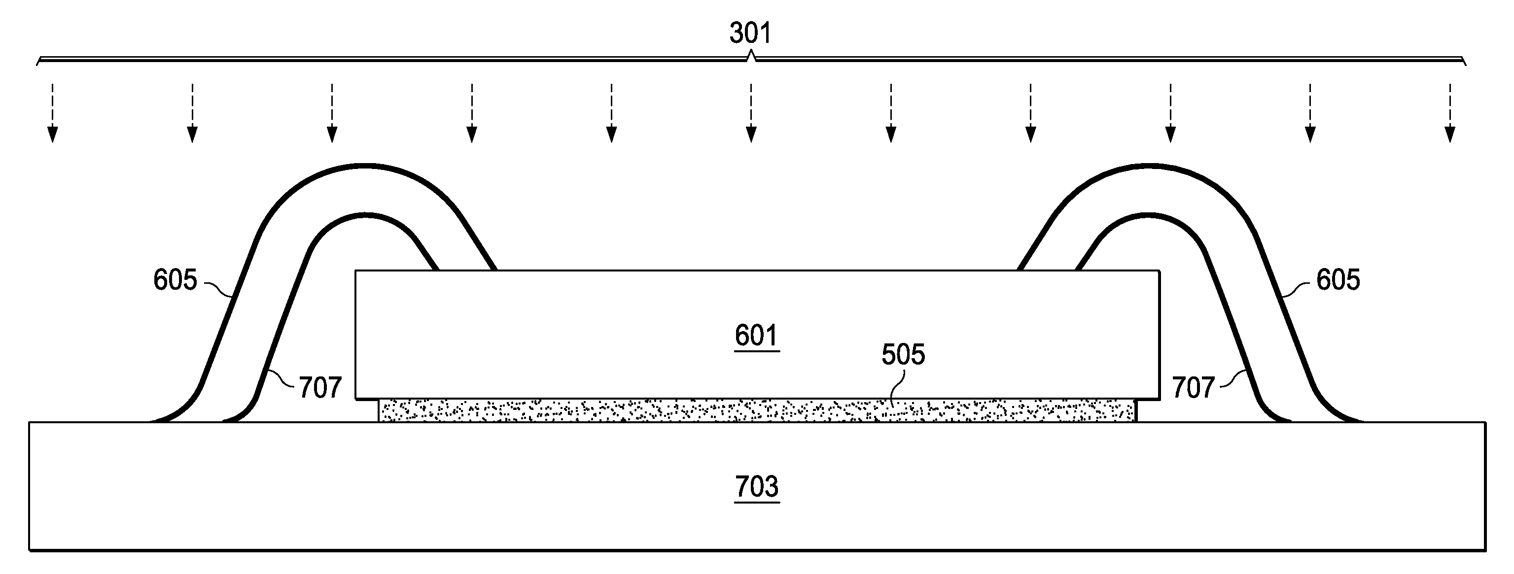
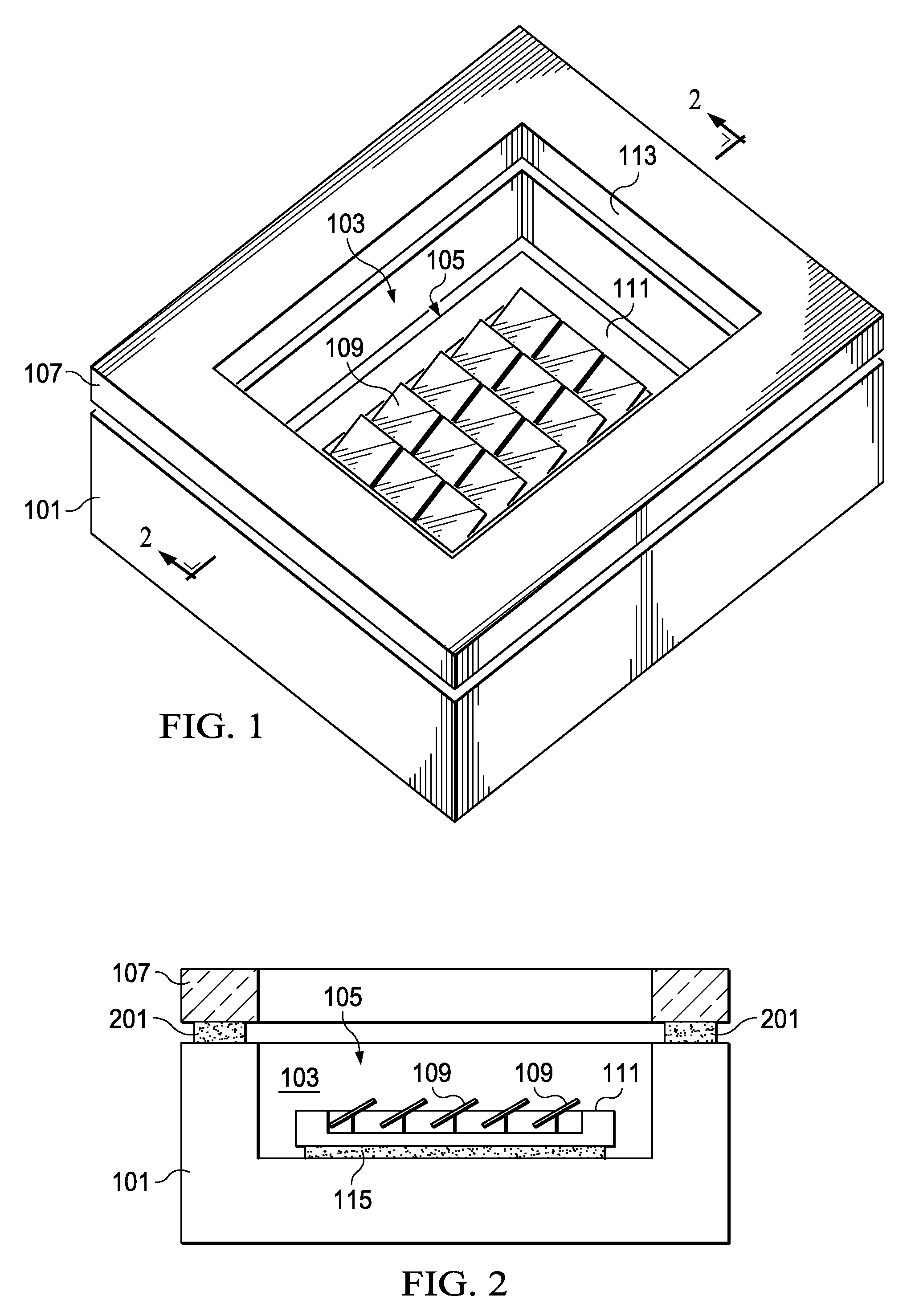
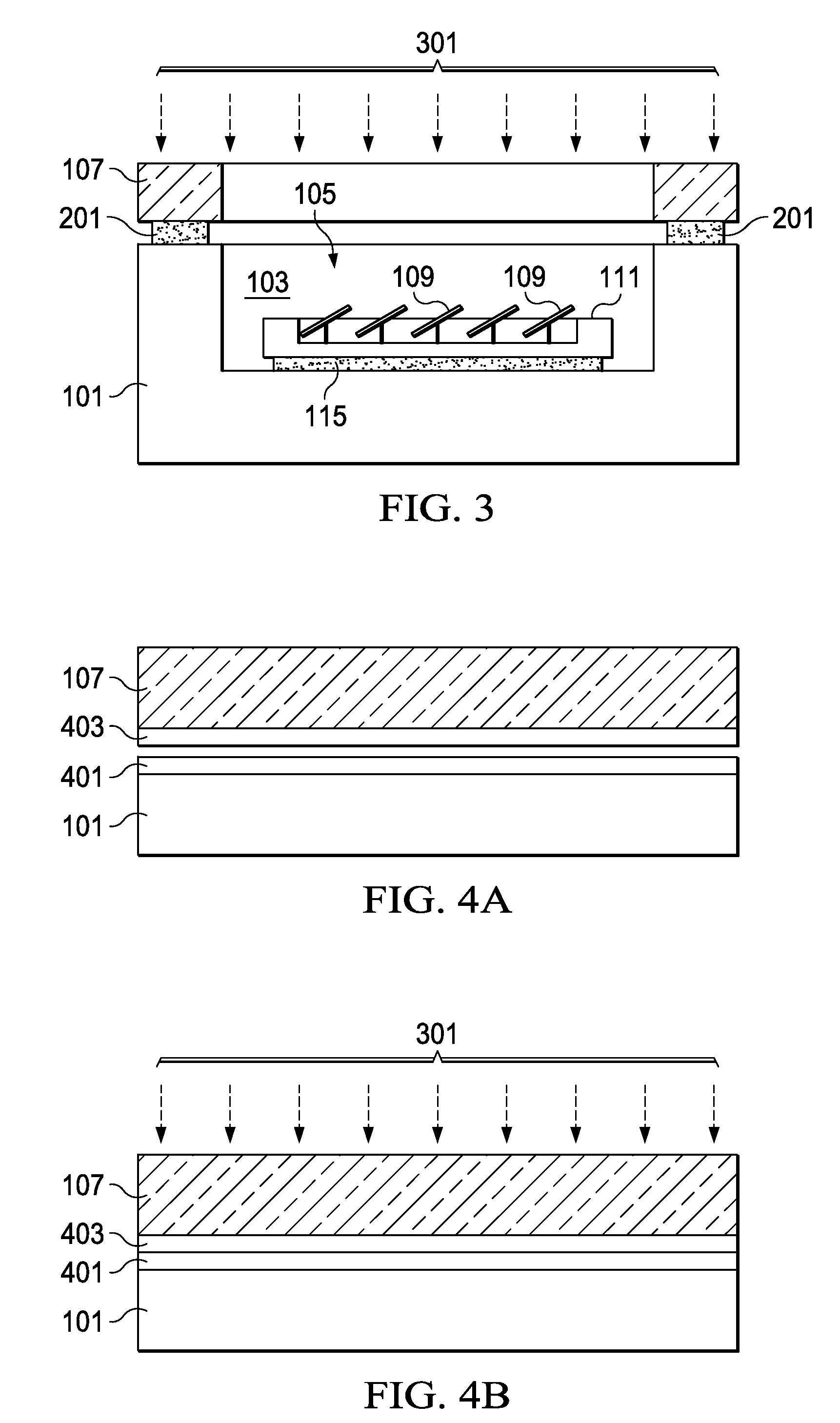
[0023]With reference now to FIG. 1, there is shown a substrate 101 with a MEMs device 105 located within a cavity 103 of the substrate 101 and enclosed by a cover 107. In a preferred embodiment, the MEMs device 105 is a digital micromirror device (D...


PUM


Abstract

A method for curing an adhesive is disclosed. A preferred embodiment comprises securing a cover onto a substrate to enclose a MEMs device using an adhesive. The adhesive is either partially or fully cured using microwave radiation. Another preferred embodiment utilizes the microwave radiation to cure an encapsulant placed to protect a semiconductor device.

Description

TECHNICAL FIELD[0001]The present invention relates generally to a system and method for manufacturing semiconductor device packages, and more particularly to a system and method for curing semiconductor device package adhesives and encapsulants.BACKGROUND[0002]Adhesives and encapsulants are used for many reasons throughout the manufacturing of semiconductor devices. For example, an adhesive may be used to seal a cover over a microelectromechanical device (MEMs device), to attach a die to a substrate or wafer, or to encapsulate and protect a wafer. Traditionally, these adhesives and encapsulants have been cured by placing the adhesive (and the rest of the structure) into an oven, and using convective heat transfer to heat and cure the adhesive.[0003]However, this thermal curing process has many problems associated with it. One of the larger problems is that by using convective heat transfer, the entire structure, and not just the material that is desired to be cured, is heated. Becau...

Claims


Application Information

Patent Timeline
Patent Type & Authority Applications(United States)
IPC IPC(8): H01L21/56H01L21/50
CPCB81B7/0048B81C1/00269H01L2924/1461H01L2224/83191H01L2924/0665H01L2924/014H01L2924/0105H01L2924/01033H01L2924/01006H01L2224/2919H01L2924/14H01L2924/07802H01L2924/01079H01L2924/01047H01L2924/01029H01L2924/01013B81C2203/0109B81C2203/038H01L21/56H01L24/48H01L24/83H01L2224/16H01L2224/29007H01L2224/32014H01L2224/32225H01L2224/48091H01L2224/48227H01L2224/73265H01L2224/83856H01L2224/83862H01L2224/83865H01L2224/83885H01L2924/00014H01L2924/00H01L2924/00012H01L2924/181H01L24/73H01L2224/45099H01L2224/45015H01L2924/207
Inventor THOMSON, GARY PHILIPSAKAKINI, PETER JOSEPH
Owner TEXAS INSTR INC
Why Eureka
Try Eureka