Eureka AIR delivers breakthrough ideas for toughest innovation challenges, trusted by R&D personnel around the world.

Wafer level package and method of fabricating the same

Inactive Publication Date: 2009-10-22
ELECTRONICS & TELECOMM RES INST
View PDF5 Cites 3 Cited by
  • Summary
  • Abstract
  • Description
  • Claims
  • Application Information

AI Technical Summary

Benefits of technology

[0011]The present invention is directed to providing a wafer level package capable of reducing production cost required for forming a communication line of an internal device of the wafer level package and the complexity of the fabrication process, and a method of fabricating the wafer level package.

Problems solved by technology

In general, devices performing specific functions, such as a Radio Frequency (RF) filter, an RF switch, a Microelectromechanical Systems (MEMS) structure and an actuator, which are manufactured in a chip unit, are vulnerable to moisture, particles and high temperature, and thus require separate packaging.
However, the via process used to form a communication line penetrating a substrate is costly, amounting to about 30 to 40% of the total fabrication cost, and complicates the process.

Method used


Image

  • Wafer level package and method of fabricating the same
  • Wafer level package and method of fabricating the same
  • Wafer level package and method of fabricating the same

Examples


Embodiment Construction

[0020]Hereinafter, exemplary embodiments of the present invention will be described in detail. However, the present invention is not limited to the embodiments disclosed below, but can be implemented in various forms. The following embodiments are described in order to enable those of ordinary skill in the art to embody and practice the present invention. Throughout the drawings and the following descriptions of exemplary embodiments, like numerals denote like elements. In the drawings, the sizes and thicknesses of layers and regions may be exaggerated for clarity.

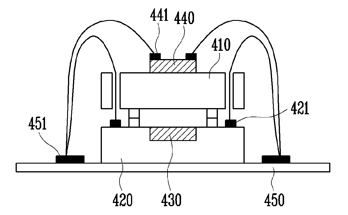
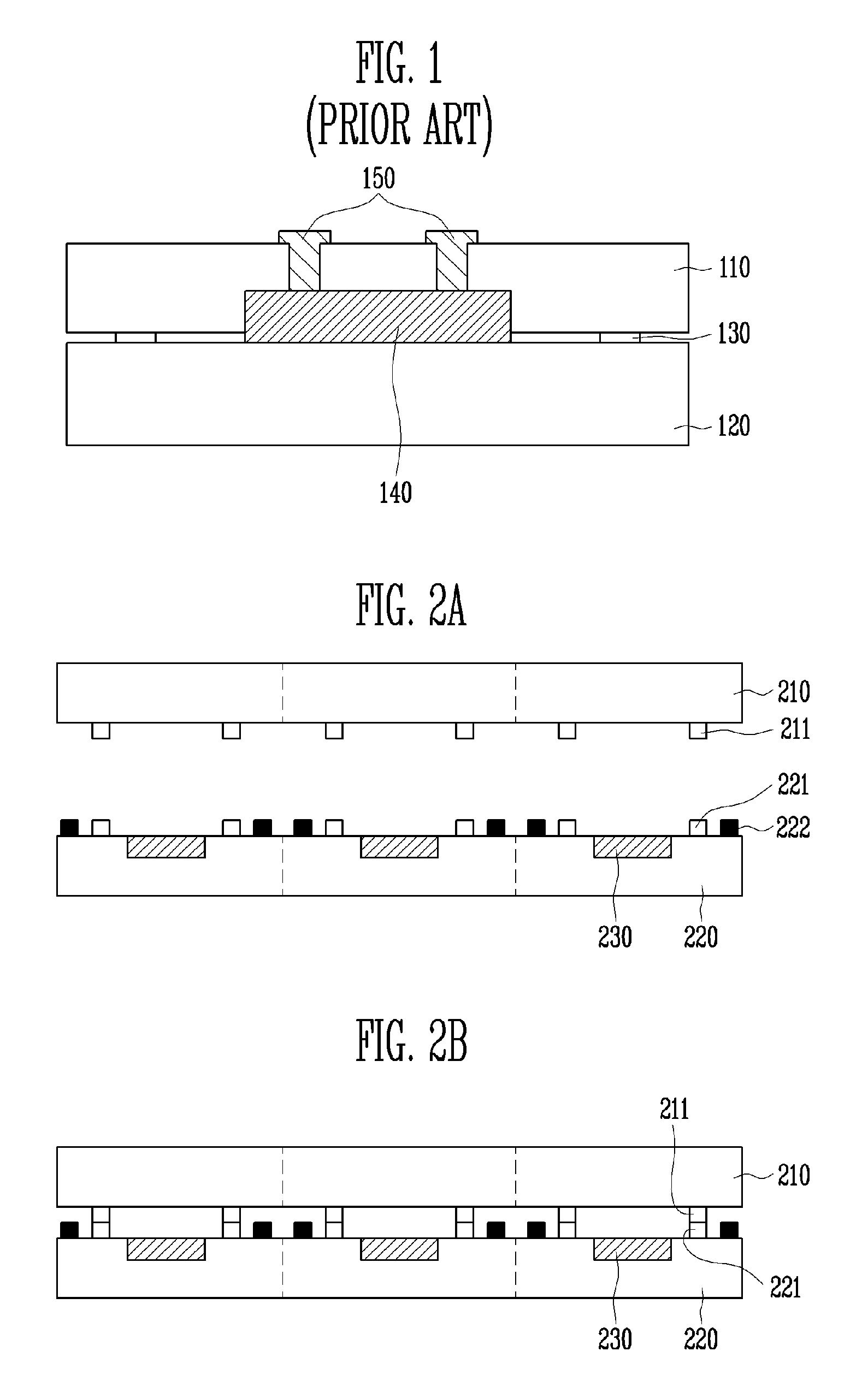
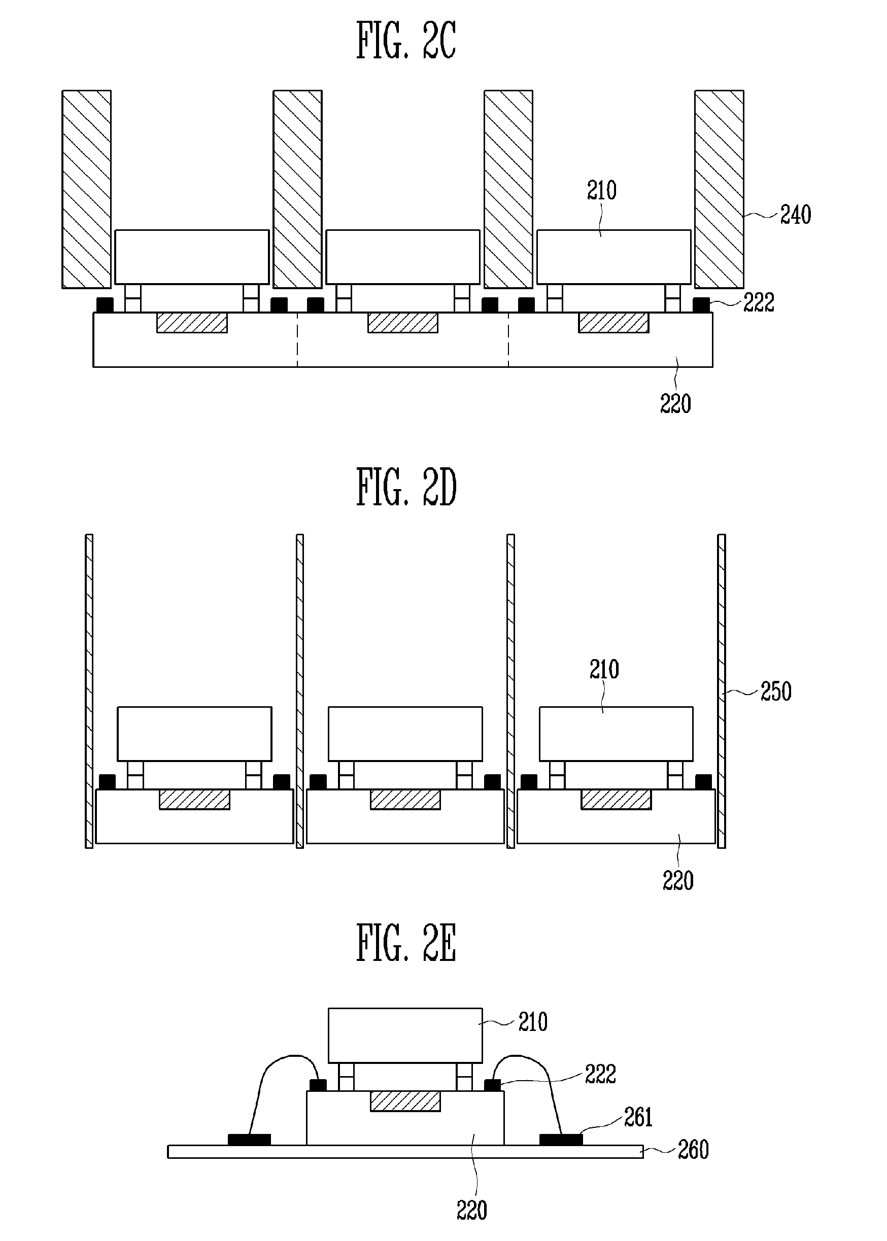
[0021]FIGS. 2A to 2E illustrate a process of fabricating a wafer level package according to a first exemplary embodiment of the present invention.

[0022]Referring to FIG. 2A, a lower substrate 220 includes cavities in which Microelectromechanical Systems (MEMS) structures 230 are disposed, and Input / Output (I / O) pads 222 electrically connected with the MEMS structures 230 are formed on the lower substrate. The I / O pads 222 ...


PUM


Abstract

Provided are a wafer level package in which a communication line can be readily formed between an internal device and the outside of the package, and a method of fabricating the wafer level package. The wafer level package includes a first substrate having a cavity in which a first internal device is disposed, an Input / Output (I / O) pad formed on the first substrate and electrically connected with the first internal device, a second substrate disposed over the first substrate and from which a part corresponding to the I / O pad is removed, and a solder bonding the first and second substrates. According to the wafer level package and the method of fabricating the same, upper and lower substrates are sawed to different cutting widths, or a hole is formed in the upper substrate, such that a communication line of an internal device can be readily formed without a via process which penetrates a substrate. Therefore, in comparison with a conventional wafer level package fabricated using the via process, it is possible to simplify a fabrication process and reduce production cost.

Description

CROSS-REFERENCE TO RELATED APPLICATION[0001]This application claims priority to and the benefit of Korean Patent Application No. 2008-35488, filed Apr. 17, 2008, the disclosure of which is incorporated herein by reference in its entirety.BACKGROUND[0002]1. Field of the Invention[0003]The present invention relates to a wafer level package and a method of fabricating the same, and more particularly, to a wafer level package in which a communication line can be readily formed between an internal device and the outside of the package, and a method of fabricating the wafer level package.[0004]2. Discussion of Related Art[0005]In general, devices performing specific functions, such as a Radio Frequency (RF) filter, an RF switch, a Microelectromechanical Systems (MEMS) structure and an actuator, which are manufactured in a chip unit, are vulnerable to moisture, particles and high temperature, and thus require separate packaging. The packaging is performed by covering and sealing an upper s...

Claims


Application Information

Patent Timeline
IPC IPC(8): H01L23/52H01L21/66H01L21/00
CPCB81B7/007B81C2203/0118H01L2924/1461H01L2224/45144H01L2924/01033H01L24/48H01L2924/01082H01L23/10H01L24/94H01L2224/16145H01L2224/48091H01L2924/01029H01L2924/01047H01L2924/01077H01L2924/01078H01L2924/01079H01L2924/00014H01L2924/00H01L24/45H01L2224/45015H01L2924/16235H01L2924/2076H01L2224/05599H01L23/48
Inventor MOON, JONG TAEEOM, YONG SUNGLEE, MIN JIYU, HYUN KYU
Owner ELECTRONICS & TELECOMM RES INST
Why Eureka
Eureka Blog
Learn More