
Light mark, method and device for light mark modulation and demodulation

a light mark and modulation technology, applied in the field of communication technology, can solve the problems of difficult identification of optical fiber connection relation, limited available frequency marks, and insufficient large-scale network, so as to reduce interference between marks with different wavelengths and power consumption of mark modulation devices.

Active Publication Date: 2009-10-22
HUAWEI TECH CO LTD
View PDF3 Cites 6 Cited by
  • Summary
  • Abstract
  • Description
  • Claims
  • Application Information

AI Technical Summary

Benefits of technology

[0041]2) As the number of required frequencies is greatly reduced, the demand for the mark modulation hardware is lowered, and the difficulty in mark demodulation is reduced, thus improving the demodulation performance.
[0043]4) As discontinuous mark frequencies are adopted, the interference between the marks with different wavelengths is reduced, and the power consumption of the mark modulation device is also lowered.

Problems solved by technology

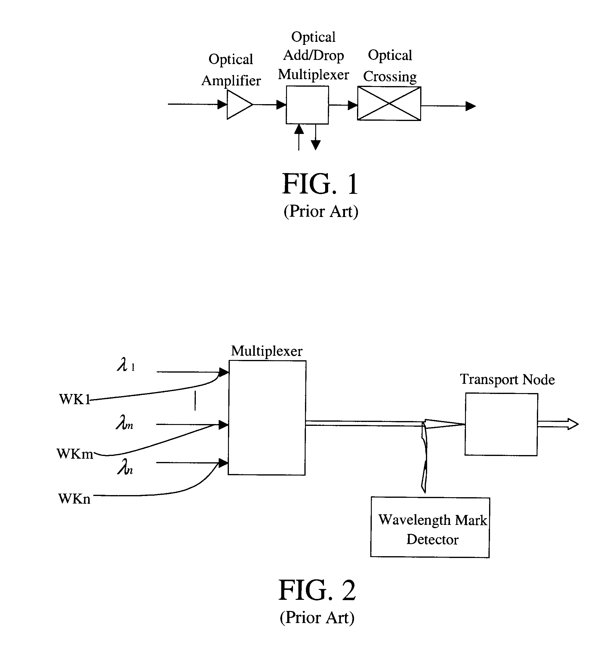
Therefore, it is difficult to identify optical fiber connection relation, trace and performance of wavelength path, and the like.
As a result, available frequency marks become very limited, and the above marks are far from being sufficient for a large-scale network.
1) Although the number of frequencies required by the unique mark for each upload wavelength in the network may be reduced by frequency combination, as the number of frequencies required by a current large-scale and high density network is still very huge, this method cannot meet the requirement of the network.
2) Under the condition of a fixed available frequency range, in order to increase the number of available frequencies, the frequency interval between adjacent available frequencies must be reduced. In order to avoid interference between adjacent frequencies, the frequency generator is required to have a higher frequency stability, which increases hardware requirements of the mark modulation end. Meanwhile, as the frequency interval between the marks is reduced, the difficulty in demodulation is increased, no matter the demodulation device employs the FFT demodulation scheme or the FIR filtering scheme.
Thereby, at the same sampling rate, more nodes need to be FFT transformed, which increases the difficulty in transformation.
Meanwhile, as the frequency interval between the marks is reduced, the interference between frequencies of adjacent marks becomes greater during the demodulation, so that interference frequencies are easily produced, and correct amplitudes of the frequencies of the marks cannot be easily obtained.
As a result, the performance of the light marking technique is degraded.
3) When a wavelength conflict occurs, the conflict may not be correctly detected, and instead, an error determination is easily made.
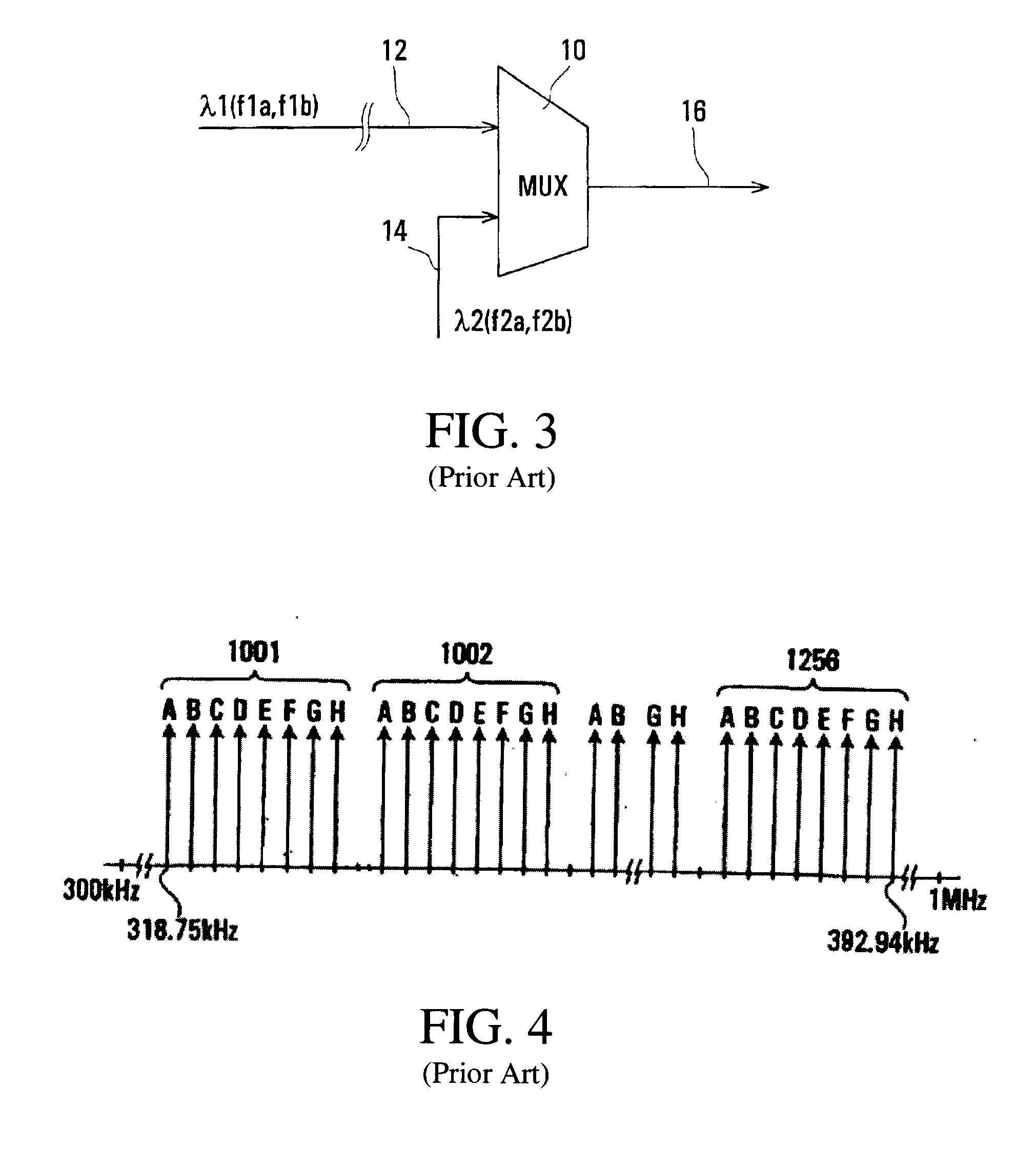
1. Each wavelength still needs more than two frequencies. The solution adopted in the industry is to modulate the mark data by 8-ary frequency shift keying (8FSK), so that each wavelength needs eight frequencies, which is still a large number.
2. In case of a wavelength conflict, the data may be confused after demodulation, and the conflict cannot be easily determined.

Method used


Image

  • Light mark, method and device for light mark modulation and demodulation
  • Light mark, method and device for light mark modulation and demodulation
  • Light mark, method and device for light mark modulation and demodulation

Examples


first embodiment

[0062]FIG. 7 is a schematic structural view of a device for light mark modulation according to the present disclosure. Referring to FIG. 7, the device includes a processor 70, a Direct Digital Synthesizer (DDS) 71, a switch 72, an amplifier 73, and a light modulator 74.

[0063]The processor is adapted to control the DDS 71 to generate a frequency mark, and control an amplification level of the frequency mark, so as to make the frequency mark meet the requirement.

[0064]The DDS 71 is connected to the processor 70, and controlled by the processor 70 to generate a corresponding frequency mark.

[0065]The switch 72 is connected to the processor 70 and the DDS 71, and controlled by the processor 70 to be turned on or off, so as to generate a mark with periodically alternating frequency and interval.

[0066]The amplifier 73, connected to the switch 72 and the processor 70, is adapted to receive the mark with periodically alternating frequency and interval, and controlled by the processor 70 to a...

second embodiment

[0074]FIG. 8 is a flow chart of a method for light mark modulation according to the present disclosure. Referring to FIG. 8, the method includes the following steps.

[0075]In Step 1, a DDS is controlled to generate a mark with periodically alternating frequency and interval.

[0076]The mark with periodically alternating frequency and interval may be generated by the DDS 71 under the control of a processor 70. Specifically, the processor 70 controls the DDS 71 to generate continuous frequency marks, and the processor 70 controls the frequency and the interval to appear in a periodically alternating manner by controlling the open or closed state of a circuit; or the processor controls the DDS 71 to directly generate the mark with periodically alternating frequency and interval.

[0077]In Step 2, the frequency mark with periodically alternating frequency and interval is amplified.

[0078]In Step 3, the frequency mark signal obtained after amplification is modulated onto an optical signal.

[007...

third embodiment

[0084]FIG. 9 is a schematic view of a device for light mark demodulation according to the present disclosure. Referring to FIG. 9, the device includes a signal receiving circuit and a digital processor 94.

[0085]The signal receiving circuit is adapted to split off a small portion of light from an optical signal modulated with a frequency mark, which is subjected to photoelectric conversion and analogue-to-digital conversion and then provided to the digital processor. The signal receiving circuit further includes a splitter 90, a photoelectric conversion unit 91, an amplifying and filtering unit 92, and an analogue-to-digital conversion unit 93.

[0086]The splitter 90 is adapted to split off a small portion of light from the optical signal modulated with the frequency mark.

[0087]The photoelectric conversion unit 91 is connected to the splitter 90, and adapted to receive the split light and photoelectrically convert the optical signal into an electrical signal.

[0088]The amplifying and fi...


PUM


Abstract

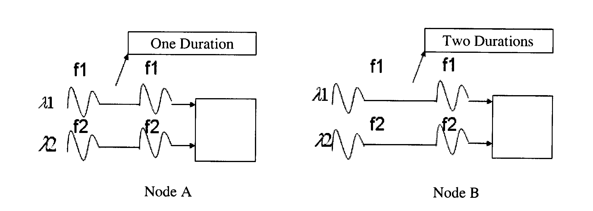
A light mark, a method and a device for light mark modulation and demodulation are disclosed. The modulation method includes: generating a mark with periodically alternating frequency and interval; and modulating the mark signal onto an optical signal. In the present disclosure, the mark with periodically alternating frequency and interval is adapted to distinguish different wavelengths by using different frequencies, and distinguish the same wavelength from different nodes by using the same frequency but different intervals. Therefore, numerous available marks are obtained with a small number of frequencies, and unique marks for all wavelengths in a network only require a number of frequencies equal to the number of the wavelengths in the network. Moreover, even if a wavelength conflict occurs, the wavelength conflict can be determined according to detected marks.

Description

CROSS-REFERENCE TO RELATED APPLICATION[0001]This application is a continuation of International Patent Application No. PCT / CN2008 / 01376, filed Jun. 20, 2008, and entitled “LIGHT MARK, METHOD AND DEVICE FOR LIGHT MARK MODULATION AND DEMODULATION,” which claims the benefit of priority to Chinese Patent Application No. 200710117634.5, filed on Jun. 20, 2007, and entitled “LIGHT MARK, METHOD AND DEVICE FOR LIGHT MARK MODULATION AND DEMODULATION”, both of which are incorporated herein by reference in their entireties.FIELD OF THE DISCLOSURE[0002]The present disclosure relates to the field of communication technology, and more particularly to a light mark, a method and a device for light mark modulation and demodulation.BACKGROUND OF THE DISCLOSURE[0003]With the development of optical transport technologies, optical transport networks develop towards configurable all-optical networks, and network topologies develop towards MESH networks, so the network size becomes larger and larger. FIG....

Claims


Application Information

Patent Timeline
Patent Type & Authority Applications(United States)
IPC IPC(8): H04B10/08
CPCH04J14/0298H04J14/0263H04J14/0276H04J14/0258
Inventor SHEN, SHUQIANG
Owner HUAWEI TECH CO LTD
Learn More