Bridges for interconnecting interposers in multi-chip integrated circuits

a technology of interconnecting interposers and bridges, which is applied in the direction of basic electric elements, solid-state devices, electrical apparatus construction details, etc., can solve the problem of limited substrate bandwidth

Active Publication Date: 2009-10-29
GLOBALFOUNDRIES US INC
View PDF4 Cites 137 Cited by
  • Summary
  • Abstract
  • Description
  • Claims
  • Application Information

AI Technical Summary

Benefits of technology

[0005]The present invention provides a structure (and a method for forming the same)

Problems solved by technology

However, the bandwidth of

Method used


Image

  • Bridges for interconnecting interposers in multi-chip integrated circuits
  • Bridges for interconnecting interposers in multi-chip integrated circuits
  • Bridges for interconnecting interposers in multi-chip integrated circuits

Examples


Embodiment Construction

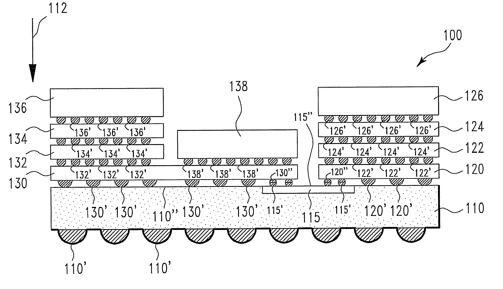
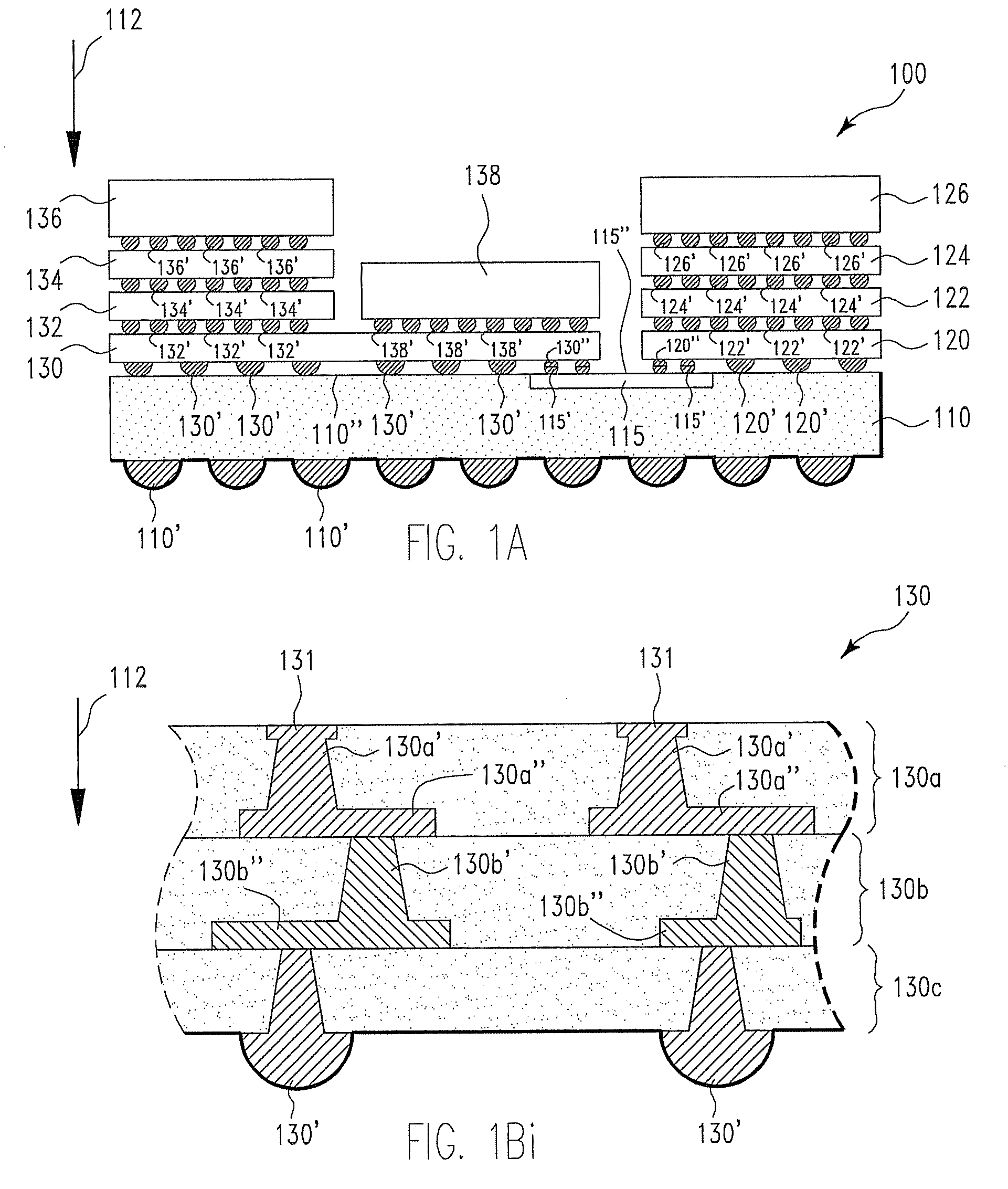
[0014]FIG. 1A shows a cross-section view of a semiconductor structure 100, in accordance with embodiments of the present invention. More specifically, with reference to FIG. 1A, the semiconductor structure 100 comprises a substrate 110, interposers 120, 122, 124, 130, 132, and 134 on the substrate 110, semiconductor chips (integrated circuits) 126, 136, and 138, and a bridge 115. In one embodiment, the semiconductor chip 136 is a microprocessor, the semiconductor chip 138 is a memory interfacing chip, and the semiconductor chip 126 is a memory chip.

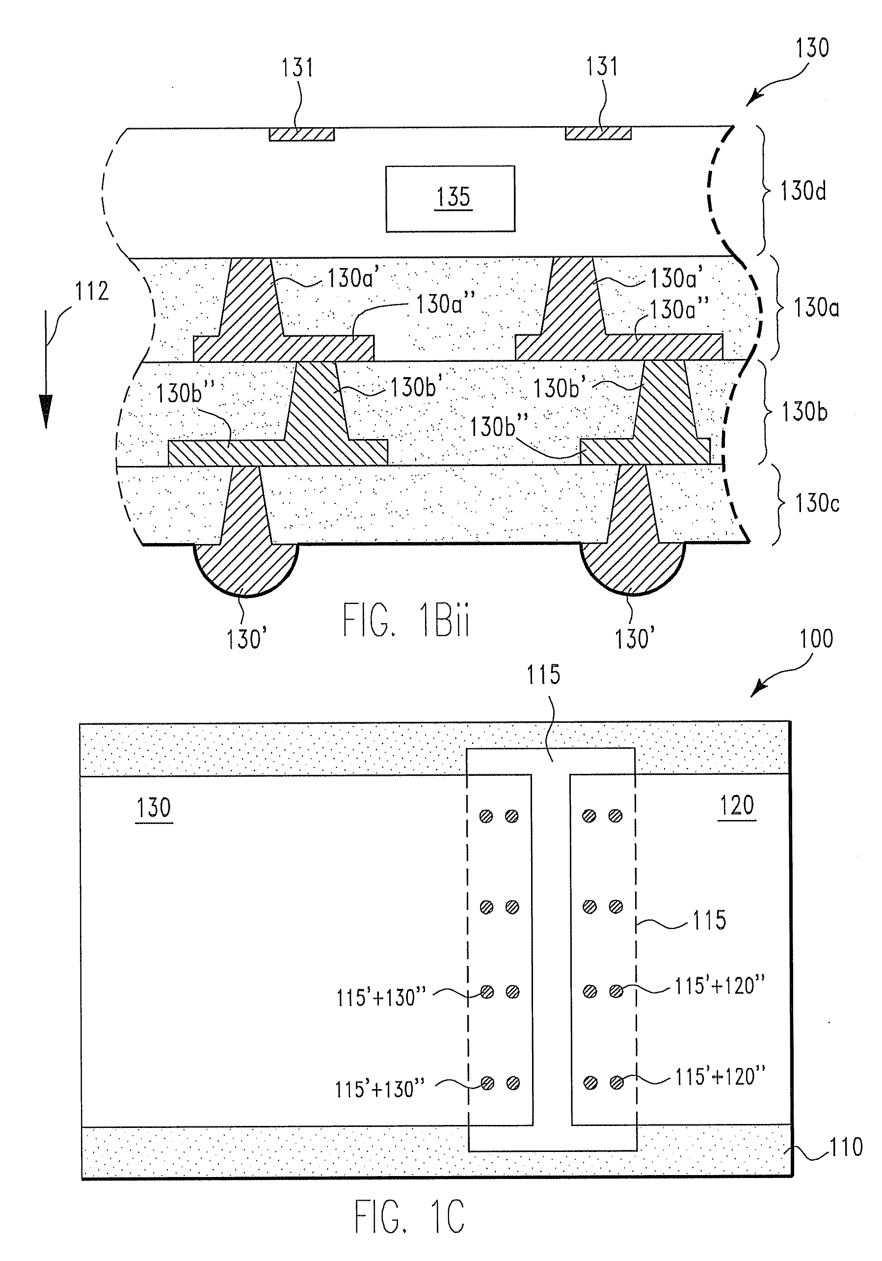
[0015]In one embodiment, the interposer 130 comprises multiple interconnect layers (not shown inFIG. 1A but can be seen in FIGS. 1Bi and 1Bii). FIG. 1Bi shows a cross-section view of a portion of the interposer 130, in accordance with embodiments of the present invention. The thickness of the interposer 130 can be less than the thickness of the wafer from which the interposer 130 is formed. For instance, the thickness of the interposer 13...


PUM


Abstract

A structure and a method for forming the same. The structure includes a substrate, a first interposer on the substrate, a second interposer on the substrate, and a first bridge. The first and second interposers are electrically connected to the substrate. The first bridge is electrically connected to the first and second interposers.

Description

[0001]This invention was made with Government support under Contract No.: H98 230-07-C-0409 awarded by RES National Security Agency. The Government has certain rights in this invention.FIELD OF THE INVENTION[0002]The present invention relates generally to multi-chip integrated circuits and more particularly to silicon bridge interconnections for interconnecting interposers in multi-chip integrated circuits.BACKGROUND OF THE INVENTION[0003]In a typical multi-chip integrated circuit, interposers may be used to electrically connect the chips to the substrate. In other words, the chips can communicate with one another via the substrate. However, the bandwidth of the substrate is limited. Therefore, there is a need for a structure (and a method for forming the same) in which more communication channels between the chips are provided than in the prior art.SUMMARY OF THE INVENTION[0004]The present invention provides a structure, comprising a substrate; a first interposer on the substrate, ...

Claims


Application Information

Patent Timeline
IPC IPC(8): H01L23/538H01L21/60
CPCH01L23/49833H01L24/16H01L2924/00013H01L25/0652H01L25/0657H01L25/18H01L2224/16H01L2225/06513H01L2225/06517H01L2225/06541H01L2225/06572H01L2924/01079H01L2924/12044H01L2924/14H01L2924/1433H01L2924/15311H01L2224/29099H01L2924/15192H01L2224/16145H01L2224/16227H01L2224/17181
Inventor JOSEPH, DOUGLAS JAMESKNICKERBOCKER, JOHN ULRICH
Owner GLOBALFOUNDRIES US INC
Why Eureka
Try Eureka